AN-6921 Ver la hoja de datos (PDF) - Fairchild Semiconductor
Número de pieza
componentes Descripción
Lista de partido
AN-6921
Fairchild Semiconductor

AN-6921 Datasheet PDF : 16 Pages
| |||
AN-6921
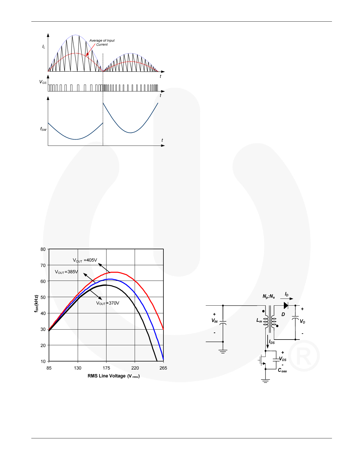
Figure 4. Frequency Variation of BCM PFC
Since the design of line filter and inductor for a BCM PFC
converter with variable switching frequency should be done
at minimum frequency condition, it is worthwhile to
examine how the minimum frequency of BCM PFC
converter changes with operating conditions.
Figure 5 shows the minimum switching frequency, which
occurs at the peak of line voltage, as a function of the RMS
line voltage for different output voltage settings. For
universal line application, the minimum switching
frequency occurs at high line (265VAC) as long as the output
voltage is lower than about 405V.
APPLICATION NOTE
3. Operation Principle of Quasi-
Resonant Flyback Converter
QR flyback converter topology can be derived from a
conventional square wave, pulse-width modulated (PWM),
flyback converter without adding additional components.
Figure 6 and Figure 7 show the simplified circuit diagram
of a quasi-resonant flyback converter and its typical
waveforms. The basic operation principles are:
During the MOSFET on time (tON), input voltage (VIN)
is applied across the primary-side inductor (Lm).
MOSFET current (IDS) increases linearly from zero to
the peak value (Ipk). During this time, the energy is
drawn from the input and stored in the inductor.
When the MOSFET is turned off, the energy stored in
the inductor forces the rectifier diode (D) to turn on.
During the diode ON time (tD), the output voltage (Vo)
is applied across the secondary-side inductor and the
diode current (ID) decreases linearly from the peak
value to zero. At the end of tD, all the energy stored in
the inductor has been delivered to the output. During
this period, the output voltage is reflected to the
primary side as Vo× Np/Ns. Then, the sum of input
voltage (VIN) and the reflected output voltage (Vo×
Np/Ns) is imposed across the MOSFET.
When the diode current reaches zero, the drain-to-
source voltage (VDS) begins to oscillate by the
resonance between the primary-side inductor (Lm) and
the MOSFET output capacitor (Coss) with an amplitude
of Vo× Np/Ns on the offset of VIN, as depicted in Figure
7. Quasi-resonant switching is achieved by turning on
the MOSFET when VDS reaches its minimum value.
This reduces the MOSFET turn-on switching loss
caused by the capacitance loading between the drain
and source of the MOSFET.
Figure 5. Minimum Switching Frequency vs.
RMS Line Voltage (L = 780µH, POUT = 100W)
Figure 6. Schematic of QR Flyback Converter
© 2010 Fairchild Semiconductor Corporation
Rev. 1.0.1 • 8/24/10
3
www.fairchildsemi.com
Share Link: