AN-6921 Ver la hoja de datos (PDF) - Fairchild Semiconductor
Número de pieza
componentes Descripción
Lista de partido
AN-6921
Fairchild Semiconductor

AN-6921 Datasheet PDF : 16 Pages
| |||
AN-6921
APPLICATION NOTE
[STEP-A4] Current Sensing Resistor for PFC
FAN6921 has pulse-by-pulse current limit function. It is
typical to set the pulse-by-current limit level at 20~30%
higher than the maximum inductor current:
RCS1
=
0.85
I L.PK (1 + KMARGIN )
(17)
where KMARGIN is the margin factor and 0.85V is the pulse-
by-pulse current limit threshold.
(Design Example) Choosing the margin factor as
35%, the sensing resistor is selected as:
RCS1
=
0.85
I L.PK (1 + KMARGIN )
=
0.85
3.14(1+ 0.35)
=
0.2Ω
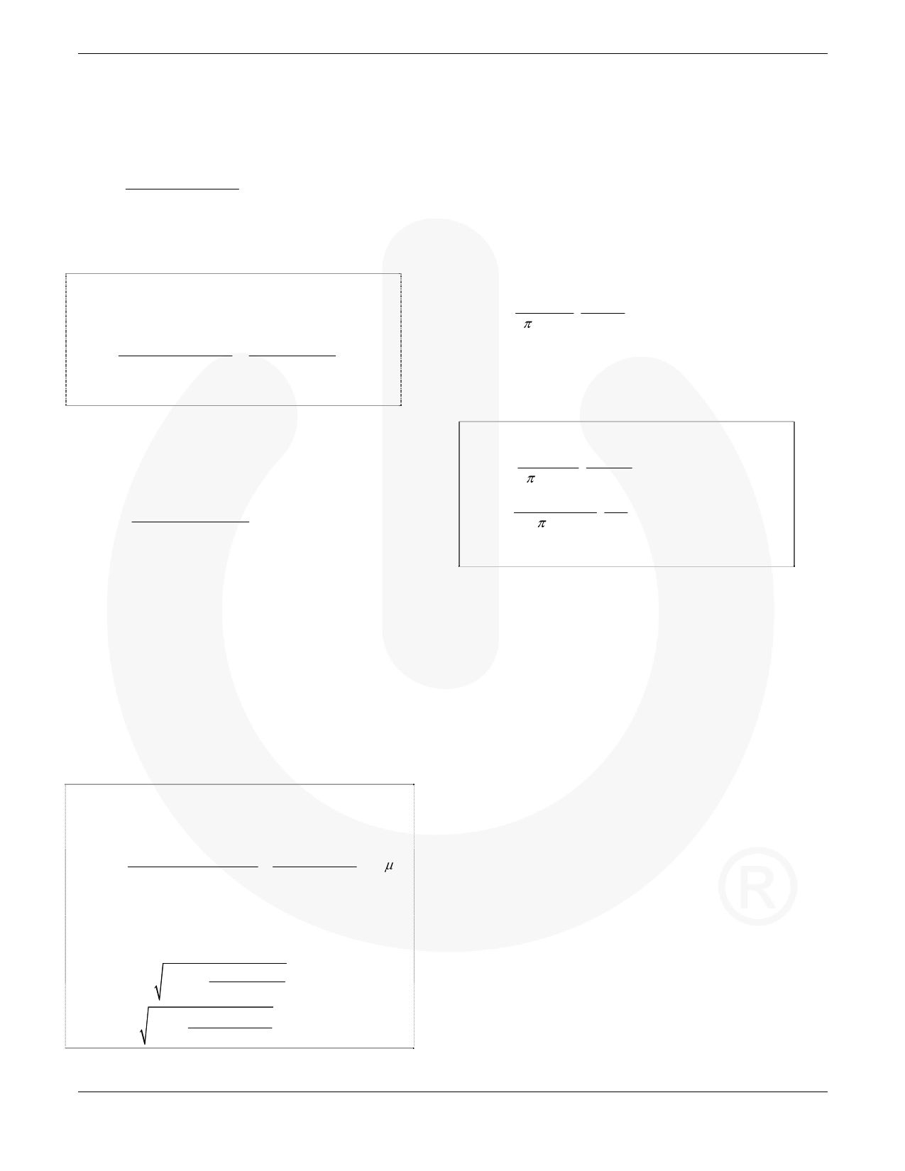
[STEP-A6] Design Compensation Network
The feedback loop bandwidth must be lower than 20Hz for
the PFC application. If the bandwidth is higher than 20Hz,
the control loop may try to reduce the 120Hz ripple of the
output voltage and the line current is distorted, decreasing
power factor. A capacitor is connected between COMP and
GND to attenuate the line frequency ripple voltage by 40dB.
If a capacitor is connected between the output of the error
amplifier and the GND, the error amplifier works as an
integrator and the error amplifier compensation capacitor
can be calculated by:
CCOMP
>
100⋅ gM
2π ⋅ 2 fLINE
⋅ 2.5
VO.PFC.H
(19)
To improve the power factor, CCOMP must be higher than the
calculated value. However, if the value is too high, the
output voltage control loop may become slow.
[STEP-A5] Output Capacitor Selection
For a given minimum PFC output voltage during the hold-
up time, the PFC output capacitor is obtained as:
CO.PFC
>
2POUT ⋅ tHOLD
V −V 2
O. PFC . L
2
O.PFC , HLD
(18)
where:
POUT is total nominal output power;
tHOLD is the required holdup time; and
VO.PFC,HLD is the allowable minimum output voltage during
the hold-up time.
For PFC output capacitor, it is typical to use 0.5~1µF per
1W output power for 400V PFC output. Meanwhile, it is
reasonable to use about 1µF per 1W output power for
variable output PFC due to the larger voltage drop during
the hold-up time than 400V output.
(Design Example)
CCOMP
>
100 ⋅ gM
2π ⋅ 2 fLINE
⋅ 2.5
VO.PFC.H
= 100 ⋅125×10−6 ⋅ 2.5 = 103nF
2π ⋅ 2⋅ 60 400
470nF is selected for better power factor.
(Design Example) Assuming the minimum
allowable PFC output voltage during the hold-up time is
160V, the capacitor should be:
CO.PFC
>
2POUT ⋅ tHOLD
VO.PFC.H 2 −VO.PFC.HLD2
=
2 ⋅90 ⋅ 20 ×10−3
2582 −1602
= 88μ F
A 100μF capacitor is selected for the output capacitor.
The minimum PFC output voltage during the hold-up
time is:
VO.PFC.HOLD =
VOUT
2
−
2POUT ⋅ tHOLD
COUT
=
2582
−
2
⋅ 90 ⋅ 20 ×10−3
100 ×10−6
= 175V
© 2010 Fairchild Semiconductor Corporation
Rev. 1.0.1 • 8/24/10
7
www.fairchildsemi.com
Share Link: