AN-6921 Ver la hoja de datos (PDF) - Fairchild Semiconductor
Número de pieza
componentes Descripción
Lista de partido
AN-6921
Fairchild Semiconductor

AN-6921 Datasheet PDF : 16 Pages
| |||
AN-6921
APPLICATION NOTE
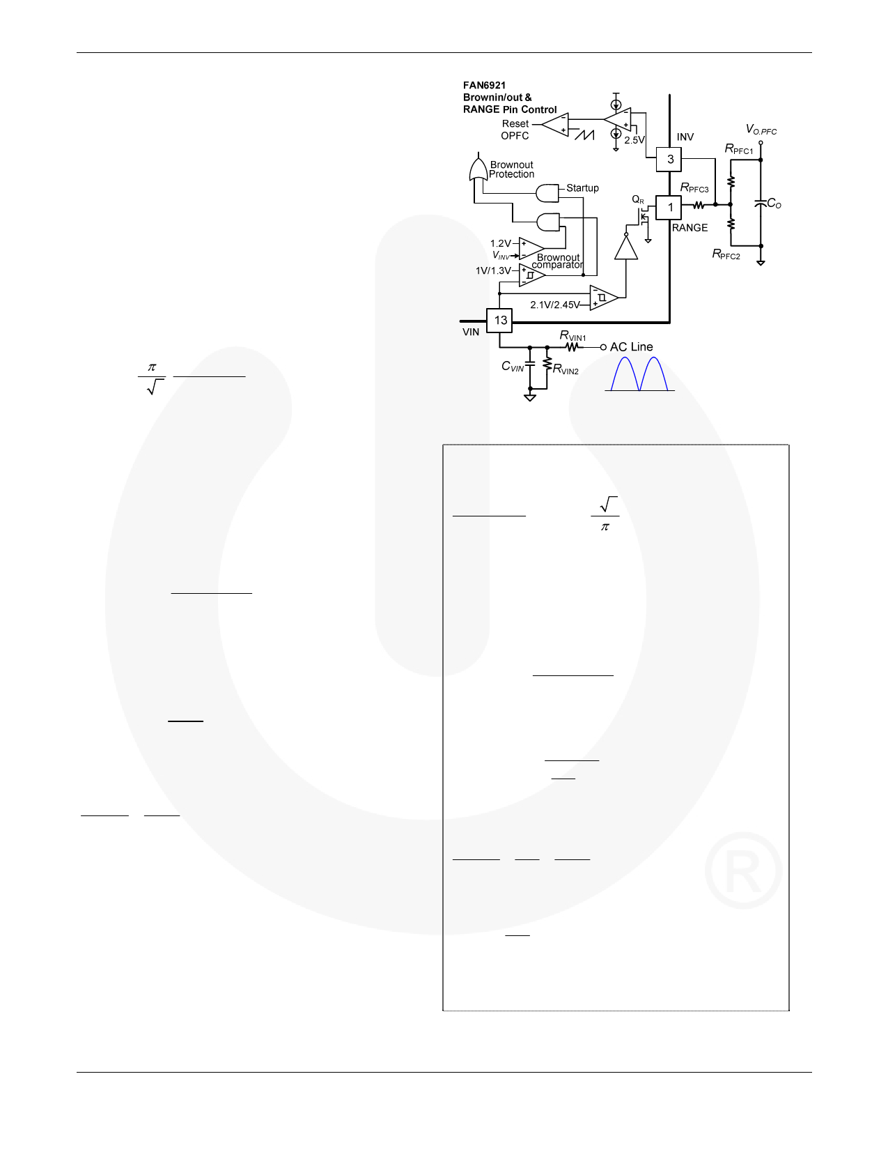
[STEP-A3] Design VIN and VO.PFC Sense Circuit
FAN6921 senses the line voltage using the averaging circuit
shown in Figure 10, where the VIN pin is connected to the
AC line through a voltage divider and low-pass filter
capacitor. When VIN pin voltage drops below 1V, the
COMP pin is clamped at 1.6V to limit the energy delivered
to output. Then VO.PFC decreases with the INV pin voltage.
When INV pin voltage drops below 1.2V, brownout
protection is triggered, stopping gate drive signals of PFC
and DC/DC. This protection is reset when VDD drops below
the turn-off threshold (UVLO threshold). When VDD rises to
the turn-on voltage after dropping below the turn-off
threshold, FAN6921 resumes normal operation (if VVIN is
higher than 1.3V).
The brownout protection level can be determined as:
VLINE.BO
=
π
22
⋅
RVIN1 + RVIN 2
RVIN 2
(12)
The minimum line voltage for PFC startup is given as:
VLINE.STR = 1.3⋅VLINE.BO
(13)
FAN6921 has a variable output voltage function that
reduces the PFC output voltage at low-line condition. When
the voltage of the VIN pin is higher than 2.45V, the internal
switch QR is turned on and the lower resistor RPFC2 of the
voltage divider is in parallel with RPFC3. Then, the PFC
output voltage for high line is given as:
VO.PFC.H
= 2.5 ⋅ ( RPFC1
RPFC 2 // RPFC3
+ 1)
(14)
When the voltage of the VIN pin is lower than 2.1V, the
lower resistor RPFC2 of the voltage divider is not in parallel
with RPFC3. Then, the PFC output voltage for low line is
given as:
VO.PFC.L
=
2.5 ⋅ ( RPFC1
RPFC 2
+ 1)
(15)
The ratio between the nominal PFC output voltage and
reduced PFC output voltage is approximated as:
VO.PFC.H ≅ RPFC 2 + 1
VO.PFCL
RPFC 3
(16)
Figure 10. VIN Sensing Internal Block
(Design Example) Setting the brownout protection trip point
as 69VAC:
RVIN1 + RVIN 2
RVIN 2
=
VLINE.BO
⋅
2
π
2
= 62
Determining RVIN2 as 154kΩ, RVIN1 is determined as 9.4MΩ.
The line voltage to start up the PFC is obtained as:
VLINE.STR = 1.3 ⋅VLINE.BO = 90VAC
To regulate the PFC output voltage at high line as 400V:
VO.PFC
= 2.5 ⋅ ( RPFC1
RPFC 2 // RPFC3
+ 1)
= 400
By selecting RPFC1=9.4MΩ:
RPFC 2
//
RPFC 3
=
9.4M Ω
( 400 −1)
=
59.1kΩ
2.5
To regulate the PFC output voltage at low line as 260V:
VO.PFC.H = 400 ≅ RPFC 2 + 1
VO.PFC.L 260 RPFC3
By selecting RPFC2=165kΩ:
RPFC 3
=
400
(
260
−1)RPFC 2
= 89kΩ
So RPFC1, RPFC2, and RPFC3 are selected from the off-the-shelf
components as 9.4MΩ, 91kΩ, and 165kΩ, respectively.
© 2010 Fairchild Semiconductor Corporation
Rev. 1.0.1 • 8/24/10
6
www.fairchildsemi.com
Share Link: