IDT72V845 Ver la hoja de datos (PDF) - Integrated Device Technology
Número de pieza
componentes Descripción
Lista de partido
IDT72V845
Integrated Device Technology

IDT72V845 Datasheet PDF : 26 Pages
| |||
IDT72V805/72V815/72V825/72V835/72V845
3.3 V CMOS DUAL SyncFIFO™ 256 x 18, 512 x 18, 1,024 x 18, 4,096 x 18
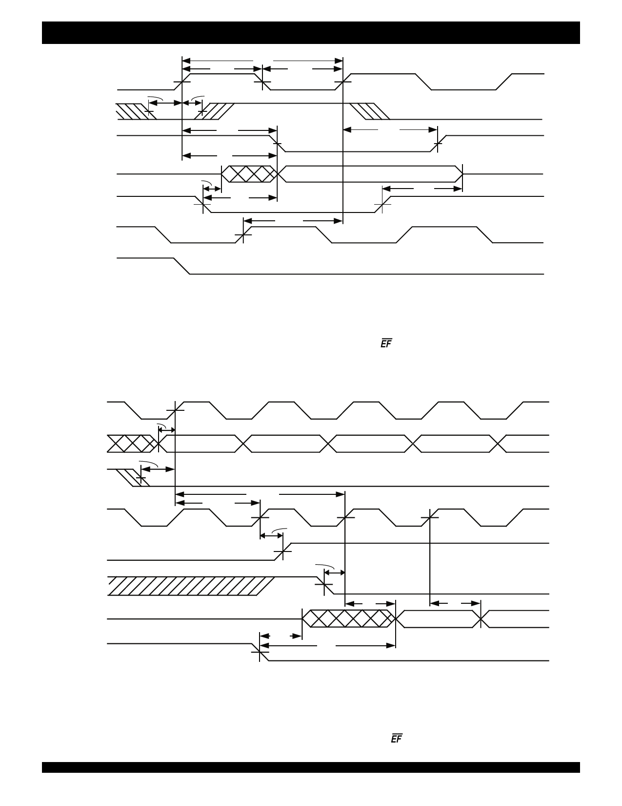
RCLK
REN
t ENS
EF
Q0 - Q17
OE
WCLK
t CLKH
t CLK
t CLKL
tENH
tREF
tA
NO OPERATION
t OLZ
t OE
tSKEW1(1)
tREF
VALID DATA
COMMERCIAL AND INDUSTRIAL
TEMPERATURE RANGES
t OHZ
WEN
4295 drw 07
NOTES:
1. tSKEW1 is the minimum time between a rising WCLK edge and a rising RCLK edge to guarantee that EF will go HIGH during the current clock cycle. If the time between
the rising edge of WCLK and the rising edge of RCLK is less than tSKEW1, then EF may not change state until the next RCLK edge.
2. Select this mode by setting (FL, RXI, WXI) = (0,0,0), (0,1,1), (1,0,0) or (1,1,1) during Reset.
Figure 7. Read Cycle Timing with Single Register-Buffered EF (IDT Standard Mode)
WCLK
t DS
D0 - D17
D0 (first valid write)
D1
D2
t ENS
WEN
tSKEW1
tFRL(1)
RCLK
t REF
EF
tENS
D3
D4
REN
tA
tA
Q0 - Q17
D0
D1
t OLZ
t OE
OE
4295 drw 08
NOTES:
1. When tSKEW1 minimum specification, tFRL (maximum) = tCLK + tSKEW1. When tSKEW1 < minimum specification, tFRL (maximum) = either 2*tCLK + tSKEW1 or tCLK + tSKEW1.
The Latency Timing applies only at the Empty Boundary (EF = LOW).
2. The first word is available the cycle after EF goes HIGH, always.
3. Select this mode by setting (FL, RXI, WXI) = (0,0,0), (0,1,1), (1,0,0) or (1,1,1) during Reset.
Figure 8. First Data Word Latency with Single Register-Buffered EF (IDT Standard Mode)
13
Share Link: