IDT72V845 Ver la hoja de datos (PDF) - Integrated Device Technology
Número de pieza
componentes Descripción
Lista de partido
IDT72V845
Integrated Device Technology

IDT72V845 Datasheet PDF : 26 Pages
| |||
IDT72V805/72V815/72V825/72V835/72V845
3.3 V CMOS DUAL SyncFIFO™ 256 x 18, 512 x 18, 1,024 x 18, 4,096 x 18
COMMERCIAL AND INDUSTRIAL
TEMPERATURE RANGES
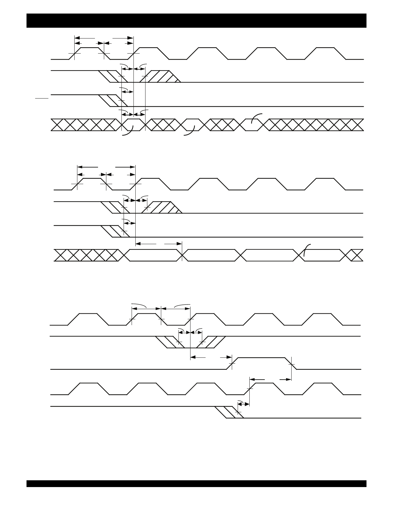
WCLK
LD
tCLK
tCLKH
tCLKL
tENS
tENS
tENH
WEN
D0—D15
tDS
PAE OFFSET
tDH
PAF OFFSET
PAE OFFSET
D0—D11
4295 drw 11
Figure 11. Write Programmable Registers (IDT Standard and FWFT Modes)
RCLK
LD
REN
Q0—Q15
tCLK
tCLKH
tCLKL
tENS
tENH
tENS
tA
UNKNOWN
PAE OFFSET
PAF OFFSET
Figure 12. Read Programmable Registers (IDT Standard Mode)
PAE OFFSET
4295 drw 12
tCLKH
tCLKL
WCLK
WEN
tENS
tENH
PAE
RCLK
n words in FIFO(2),
n + 1 words in FIFO(3)
tPAEA
n + 1 words in FIFO(2),
n + 2 words in FIFO(3)
tPAEA
n words in FIFO(2),
n + 1 words in FIFO(3)
tENS
REN
NOTES:
1. n = PAE offset.
2. For IDT Standard Mode.
3. For FWFT Mode.
4. PAE is asserted LOW on RCLK transition and reset to HIGH on WCLK transition.
5. Select this mode by setting (FL, RXI, WXI) = (0,0,0), (0,0,1), (0,1,0), (0,1,1) or (1,1,1) during Reset.
4295 drw 13
Figure 13. Asynchronous Programmable Almost-Empty Flag Timing (IDT Standard and FWFT Modes)
15
Share Link: