RTL8101 Ver la hoja de datos (PDF) - Unspecified
Número de pieza
componentes Descripción
Lista de partido
RTL8101 Datasheet PDF : 68 Pages
| |||
(Offset 0052h, R/W)
Bit
R/W
Symbol
7-6
R/W
LEDS1-0
5
R/W
DVRLOAD
4
R/W
LWACT
3
R
MEMMAP
2
R
IOMAP
1
R/W
VPD
0
R/W
PMEn
RTL8101L
Description
Refer to LED PIN definition. These bits initial value come from 93C46.
Driver Load: Software may use this bit to make sure that the driver has been
loaded. Writing 1 is 1. Writing 0 is 0. When the command register bits IOEN,
MEMEN, and BMEN of the PCI configuration space are written, the RTL8101L
will clear this bit automatically.
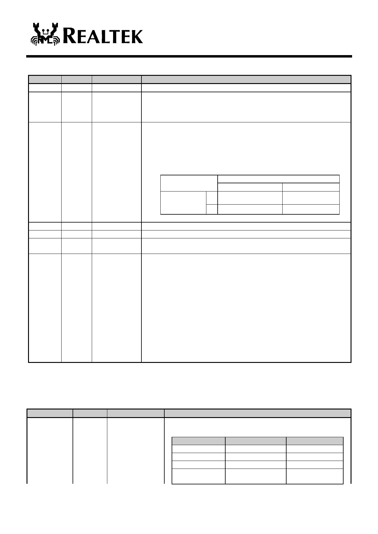
LWAKE active mode: The LWACT bit and LWPTN bit in CONFIG4 register
are used to program the LWAKE pin’s output signal. According to the
combination of these two bits, there may be 4 choices of LWAKE signal, i.e.,
active high, active low, positive (high) pulse, and negative (low) pulse. The output
pulse width is about 150ms.
The default value of each of these two bits is 0, i.e., the default output signal of
LWAKE pin is an active high signal.
LWAKE output
LWACT
0
1
0
Active high*
Active low
LWPTN
1
Positive pulse
Negative pulse
* Default value.
Memory Mapping: The operational registers are mapped into PCI memory space.
I/O Mapping: The operational registers are mapped into PCI I/O space.
Set to enable Vital Product Data: The VPD data is stored in 93C46 from within
offset 40h-7Fh.
Power Management Enable:
Writable only when 93C46CR register EEM1=EEM0=1
Let A denote the New_Cap bit (bit 4 of the Status Register) in the PCI
Configuration space offset 06H.
Let B denote the Cap_Ptr register in the PCI Configuration space offset 34H.
Let C denote the Cap_ID (power management) register in the PCI Configuration
space offset 50H.
Let D denote the power management registers in the PCI Configuration space
offset from 52H to 57H.
Let E denote the Next_Ptr (power management) register in the PCI Configuration
space offset 51H.
PMEn Description
0 A=B=C=E=0, D not valid
1 A=1, B=50h, C=01h, D valid, E=0
5.12 Media Status Register
(Offset 0058h, R/W)
Bit
R/W
Symbol
7
R/W
TXFCE/
LdTXFCE
Description
Tx Flow Control Enable: The flow control is valid in full-duplex mode
only. This register’s default value comes from 93C46.
RTL8101L
ANE = 1
ANE = 1
ANE = 1
ANE = 0 &
full-duplex mode
Remote
NWAY FLY mode
NWAY mode only
No NWAY
-
TXFCE/LdTXFCE
R/O
R/W
R/W
R/W
2003-05-28
21
Rev.1.3
Share Link: 