UPD72870 Ver la hoja de datos (PDF) - NEC => Renesas Technology
Número de pieza
componentes Descripción
Lista de partido
UPD72870 Datasheet PDF : 48 Pages
| |||
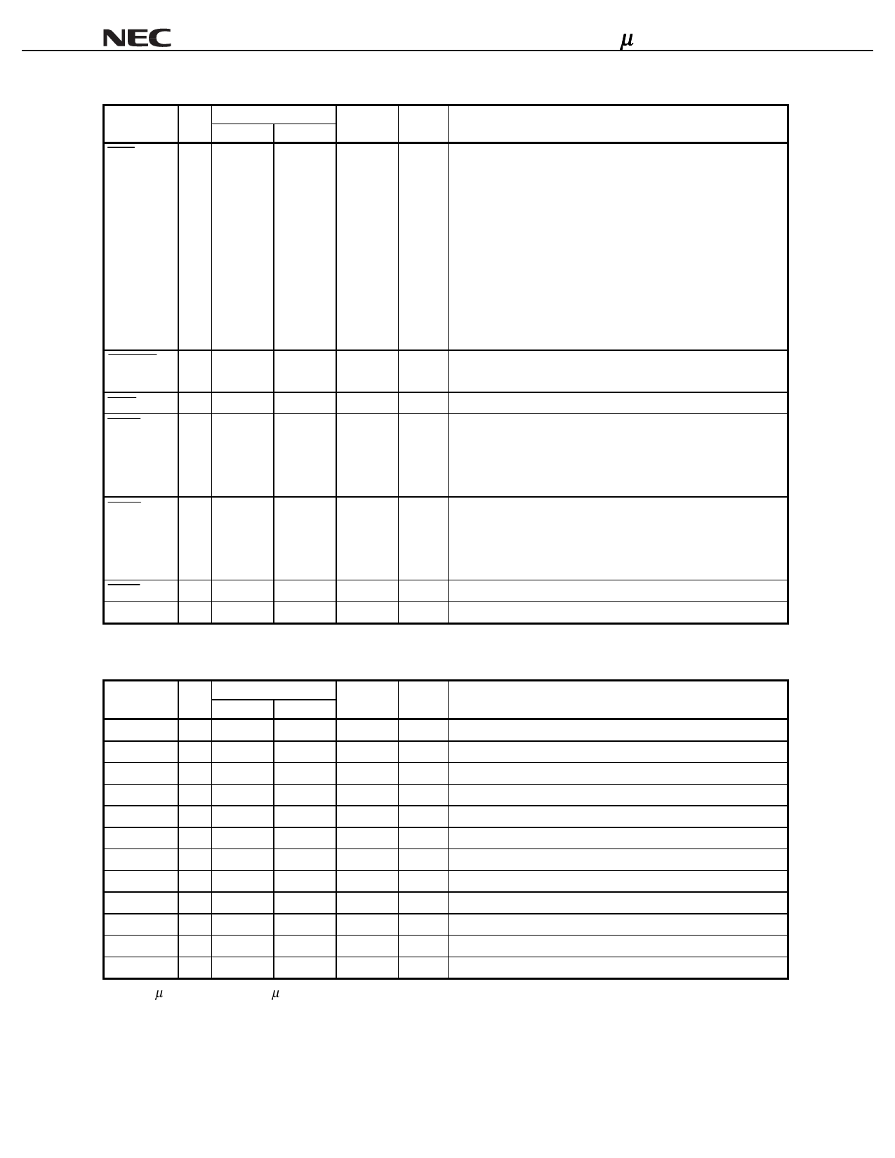
µPD72870,72871
Name
PME
5
I/O
Pin No.
LQFP FPBGA
IOL
Volts(V)
Function
O3
B2
PCI/Cardbus 5/3.3 PME Output for power management enable.
(2/2)
Caution The PME pin is not an N-channel open drain
structure pin.
Therefore, when using S3, S4, S5 state in ACPI, a
circuit that can separate between the power supply
and the PME pin externally is needed.
CLKRUN
I/O 2
INTA
PERR
O4
I/O 43
SERR
O 44
PRST
PCLK
I5
I6
ACPI: Advanced Configuration and Power Interface.
Please refer to ACPI Specification.
A1
PCI/Cardbus 5/3.3 PCICLK Running as input, to determine the status of PCLK;
as output, to request starting or speeding up clock.
B1
PCI/Cardbus 5/3.3 Interrupt the PCI interrupt request A.
R3
PCI/Cardbus 5/3.3 Parity Error is used for reporting data parity errors during all
PCI transactions, except a Special Cycle. It is an output when
AD0-AD31 and PAR are both inputs. It is an input when AD0-
AD31 and PAR are both outputs.
T3
PCI/Cardbus 5/3.3 System Error is used for reporting address parity errors, data
parity errors during the Special Cycle, or any other system error
where the effect can be catastrophic. When reporting address
parity errors, it is an output.
C2
-
5/3.3 Reset PCI reset
C1
-
5/3.3 PCI Clock 33 MHz systembus clock.
1.2 Cable Interface Signals: (15 pins)
Name
I/O
Pin No.
LQFP FPBGA
IOL
Volts(V)
Function
TpA0p
I/O 140
B8
-
- Port-1 Twisted Pair A Positive Input/Output Note 2
TpA0n
I/O 139
A8
-
- Port-1 Twisted Pair A Negative Input/Output Note 2
TpB0p
I/O 138
B9
-
- Port-1 Twisted Pair B Positive Input/Output Note 2
TpB0n
I/O 137
A9
-
- Port-1 Twisted Pair B Negative Input/Output Note 2
TpA1p Note 1 I/O 136
B10
-
- Port-2 Twisted Pair A Positive Input/Output Note 2
TpA1n Note 1 I/O 135
A10
-
- Port-2 Twisted Pair A Negative Input/Output Note 2
TpB1p Note 1 I/O 134
B11
-
- Port-2 Twisted Pair B Positive Input/Output Note 2
TpB1n Note 1 I/O 133
A11
-
- Port-2 Twisted Pair B Negative Input/Output Note 2
TpA2p Note 1 I/O 132
B12
-
- Port-3 Twisted Pair A Positive Input/Output Note 2
TpA2n Note 1 I/O 131
A12
-
- Port-3 Twisted Pair A Negative Input/Output Note 2
TpB2p Note 1 I/O 130
B13
-
- Port-3 Twisted Pair B Positive Input/Output Note 2
TpB2n Note 1 I/O 129
A13
-
- Port-3 Twisted Pair B Negative Input/Output Note 2
Note 1. µPD72870 only. In µPD72871, it is open.
2. If unused port, please refer to 4.1.4 Unused Port.
(1/2)
14
Preliminary Data Sheet S13925EJ2V0DS00
Share Link: 