ADM1023 Ver la hoja de datos (PDF) - Analog Devices
Número de pieza
componentes Descripción
Lista de partido
ADM1023 Datasheet PDF : 12 Pages
| |||
ADM1023
ABSOLUTE MAXIMUM RATINGS*
Positive Supply Voltage (VDD) to GND . . . . . . –0.3 V to +6 V
D+, ADD0, ADD1 . . . . . . . . . . . . . . . –0.3 V to VDD + 0.3 V
D– to GND . . . . . . . . . . . . . . . . . . . . . . . . . . –0.3 V to +0.6 V
SCLK, SDATA, ALERT, STBY . . . . . . . . . . . –0.3 V to +6 V
Input Current . . . . . . . . . . . . . . . . . . . . . . . . . . . . . . ± 50 mA
Input Current, D– . . . . . . . . . . . . . . . . . . . . . . . . . . . . ± 1 mA
ESD Rating, all pins (Human Body Model) . . . . . . . . 2000 V
Continuous Power Dissipation
Up to 70°C . . . . . . . . . . . . . . . . . . . . . . . . . . . . . . 650 mW
Derating Above 70°C . . . . . . . . . . . . . . . . . . . . . 6.7 mW/°C
Operating Temperature Range . . . . . . . . . . –55°C to +125°C
Maximum Junction Temperature (TJ max) . . . . . . . . . . 150°C
Storage Temperature Range . . . . . . . . . . . . –65°C to +150°C
Lead Temperature (Soldering 10 sec) . . . . . . . . . . . . . . 300°C
IR Reflow Peak Temperature . . . . . . . . . . . . . . . . . . . . . 220°C
*Stresses above those listed under Absolute Maximum Ratings may cause perma-
nent damage to the device. This is a stress rating only; functional operation of the
device at these or any other conditions above those indicated in the operational
section of this specification is not implied. Exposure to absolute maximum rating
conditions for extended periods may affect device reliability.
THERMAL CHARACTERISTICS
16-Lead QSOP Package
θJA = 105°C/W
θJC = 39°C/W
ORDERING GUIDE
Model
ADM1023ARQ
Temperature
Range
0°C to 120°C
Package
Description
16-Lead QSOP
Package
Option
RQ-16
Pin No.
1, 5, 9,
13, 16
2
3
4
6
7, 8
10
11
12
14
15
PIN FUNCTION DESCRIPTIONS
Mnemonic Description
NC
No Connect.
VDD
D+
D–
ADD1
GND
ADD0
ALERT
SDATA
SCLK
STBY
Positive supply, 3 V to 5.5 V.
Positive connection to remote tem-
perature sensor.
Negative connection to remote tem-
perature sensor.
Three-state logic input, higher bit of
device address.
Supply 0 V connection.
Three-state logic input, lower bit of
device address.
Open-drain logic output used as
interrupt or SMBus alert.
Logic input/output, SMBus serial
data. Open-drain output.
Logic input, SMBus serial clock.
Logic input selecting normal opera-
tion (high) or standby mode (low).
PIN CONFIGURATION
NC 1
16 NC
VDD 2
15 STBY
D+ 3
14 SCLK
D– 4 ADM1023 13 NC
TOP VIEW
NC 5 (Not to Scale) 12 SDATA
ADD1 6
11 ALERT
GND 7
10 ADD0
GND 8
9 NC
NC = NO CONNECT
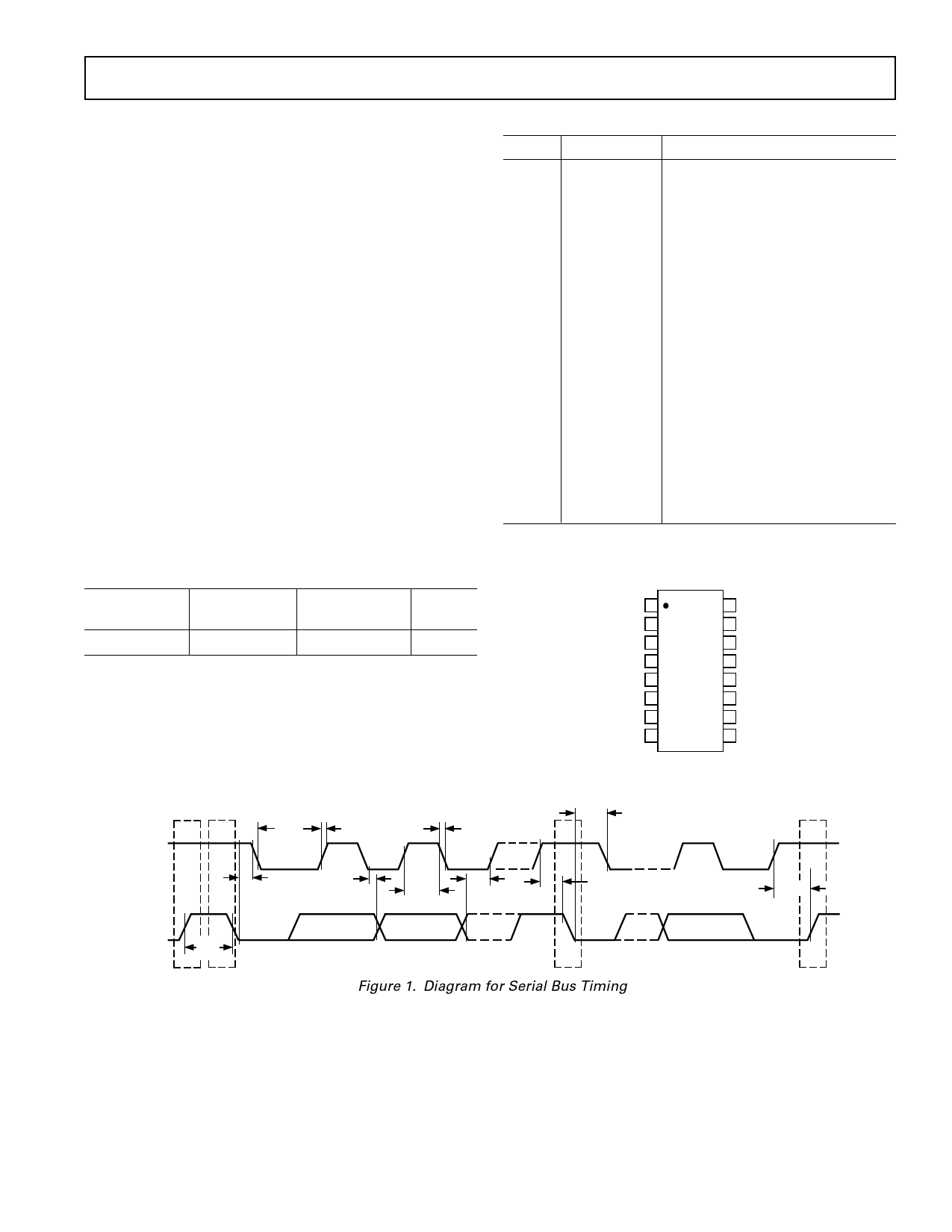
SCL
tLOW
tHD;STA
SDA
tBUF
P
S
tR
tF
tHD;DAT
tHIGH
tSU;DAT
tHD;STA
tSU;STA
S
Figure 1. Diagram for Serial Bus Timing
tSU;STO
P
REV. A
–3–
Share Link: 