ADL5390ACPZ-WP Ver la hoja de datos (PDF) - Analog Devices
Número de pieza
componentes Descripción
Lista de partido
ADL5390ACPZ-WP Datasheet PDF : 24 Pages
| |||
ADL5390
GENERALIZED MODULATOR
The ADL5390 can be configured as a traditional IQ quadrature
modulator or as a linear vector modulator by applying signals
that are in quadrature to the RF/IF input channels. Since the
quadrature generation is performed externally, its accuracy and
bandwidth are determined by the user. The user-defined band-
width is attractive for multioctave or lower IF applications
where on-chip, high accuracy quadrature generation is tradi-
tionally difficult or impractical. The gain control pins (IBBP/M
and QBBP/M) become the in-phase (I) and quadrature (Q) base-
band inputs for the quadrature modulator and the gain/phase
control for the vector modulator. The wide modulation band-
widths of the gain control interface allow for high fidelity base-
band signals to be generated for the quadrature modulator and
for high speed gain and phase adjustments to be generated for
the vector modulator.
RF/IF signals can be introduce to the ADL5390 in quadrature
by using a two-way 90o power splitter such as the Mini-Circuits
QCN-12. Each output of an ideal 90o power splitter is 3 dB
smaller than the input and has a 90o phase difference from the
other output. In reality, the 90o power splitter will have its own
insertion loss, which can be different for each output, causing a
magnitude imbalance. Furthermore, quadrature output will not
be maintained over a large frequency range, introducing a phase
imbalance. The type of 90o power splitter that should be used
for a particular application will be determined by the frequency,
bandwidth, and accuracy needed. In some applications minor
magnitude and phase imbalances can be adjusted for in the
I/Q gain control inputs.
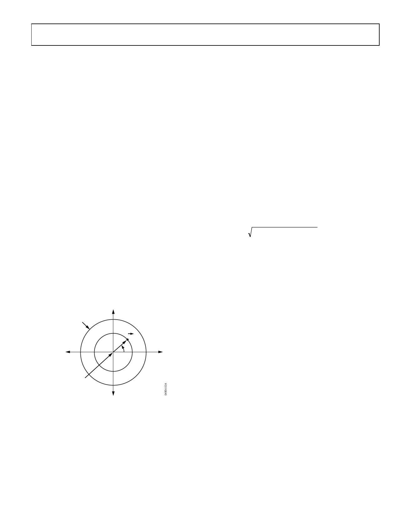
VECTOR MODULATOR
Vq
+0.5
MAX GAIN = 5dB
A
|A|
θ
–0.5
+0.5 Vi
MIN GAIN < –30dB
–0.5
Figure 34. Vector Gain Representation
The ADL5390 can be used as a vector modulator by driving the
RF I and Q inputs single-ended through a 90o power splitter. By
controlling the relative amounts of I and Q components that are
summed, continuous magnitude and phase control of the gain
is possible. Consider the vector gain representation of the
ADL5390 expressed in polar form in Figure 34. The attenuation
factors for the RF I and Q signal components are represented on
the x-axis and y-axis, respectively, by the baseband gain control
inputs VIBB and VQBB. The resultant of their vector sum represents
the vector gain, which can also be expressed as a magnitude and
phase. By applying different combinations of baseband inputs,
any vector gain within the unit circle can be programmed. The
magnitude and phase (with respect to 90o) accuracy of the 90o
power splitter will directly affect this representation and could
be seen as an offset and skew of the circle.
A change in sign of VIBB or VQBB can be viewed as a change in
sign of the gain or as a 180° phase change. The outermost circle
represents the maximum gain magnitude. The circle origin
implies, in theory, a gain of 0. In practice, circuit mismatches
and unavoidable signal feedthrough limit the minimum gain to
approximately −30 dB. The phase angle between the resultant
gain vector and the positive x-axis is defined as the phase shift.
Note that there is a nominal, systematic insertion phase through
the ADL5390 to which the phase shift is added. In the following
discussions, the systematic insertion phase is normalized to 0°.
The correspondence between the desired gain and phase and
the Cartesian inputs VIBB and VQBB is given by simple trigono-
metric identities
[ ( ) ] ( ) Gain = VIBB /VO 2 + VQBB /VO 2
( ) Phase = arctan VQBB /VIBB
where:
VO is the baseband scaling constant (285 mV).
VIBB and VQBB are the differential I and Q baseband voltages
centered around 500 mV, respectively (VIBB = VIBBP − VIBBM;
VQBB = VQBBP − VQBBM).
Note that when evaluating the arctangent function, the proper
phase quadrant must be selected. For example, if the principal
value of the arctangent (known as arctangent(x)) is used, quad-
rants 2 and 3 would be interpreted mistakenly as quadrants 4
and 1, respectively. In general, both VIBB and VQBB are needed in
concert to modulate the gain and the phase.
Pure amplitude modulation is represented by radial movement
of the gain vector tip at a fixed angle, while pure phase modula-
tion is represented by rotation of the tip around the circle at a
fixed radius. Unlike traditional I-Q modulators, the ADL5390 is
designed to have a linear RF signal path from input to output.
Traditional I-Q modulators provide a limited LO carrier path
through which any amplitude information is removed.
VECTOR MODULATOR EXAMPLE—CDMA2000
The ADL5390 can be used as a vector modulator by driving the
RF I and Q inputs (INPI and INPQ) single-ended through a 90o
power splitter and controlling the magnitude and phase using
the gain control inputs. To demonstrate operation as a vector
modulator, an 880 MHz single-carrier CDMA2000 test model
signal (forward pilot, sync, paging, and six traffic as per
Rev. 0 | Page 15 of 24
Share Link: 