ADL5390ACPZ-WP Ver la hoja de datos (PDF) - Analog Devices
Número de pieza
componentes Descripción
Lista de partido
ADL5390ACPZ-WP Datasheet PDF : 24 Pages
| |||
QUADRATURE MODULATOR
The ADL5390 can be used as a quadrature modulator by driving
the RF I and Q inputs (INPI and INPQ) single-ended through a
90o phase splitter to serve as the LO input. I/Q modulation is
applied to the baseband I and Q gain control inputs (IBBP/IBBM
and QBBP/QBBM). A simplified schematic is shown in Figure
38.
I DATA
LO IN
50Ω
SUM
PORT
PORT 1
QCN-12
TERM
PORT
PORT 2
90° PHASE
SPLITTER
10nF
INPI
66.5Ω
10nF
66.5Ω
INPQ
ADL5390
10nF 1
5
RFOM
RFOP
10nF
3
4
ETC1-1-13
(M/A-COM)
ROFP
Q DATA
Figure 38. Quadrature Modulator Application
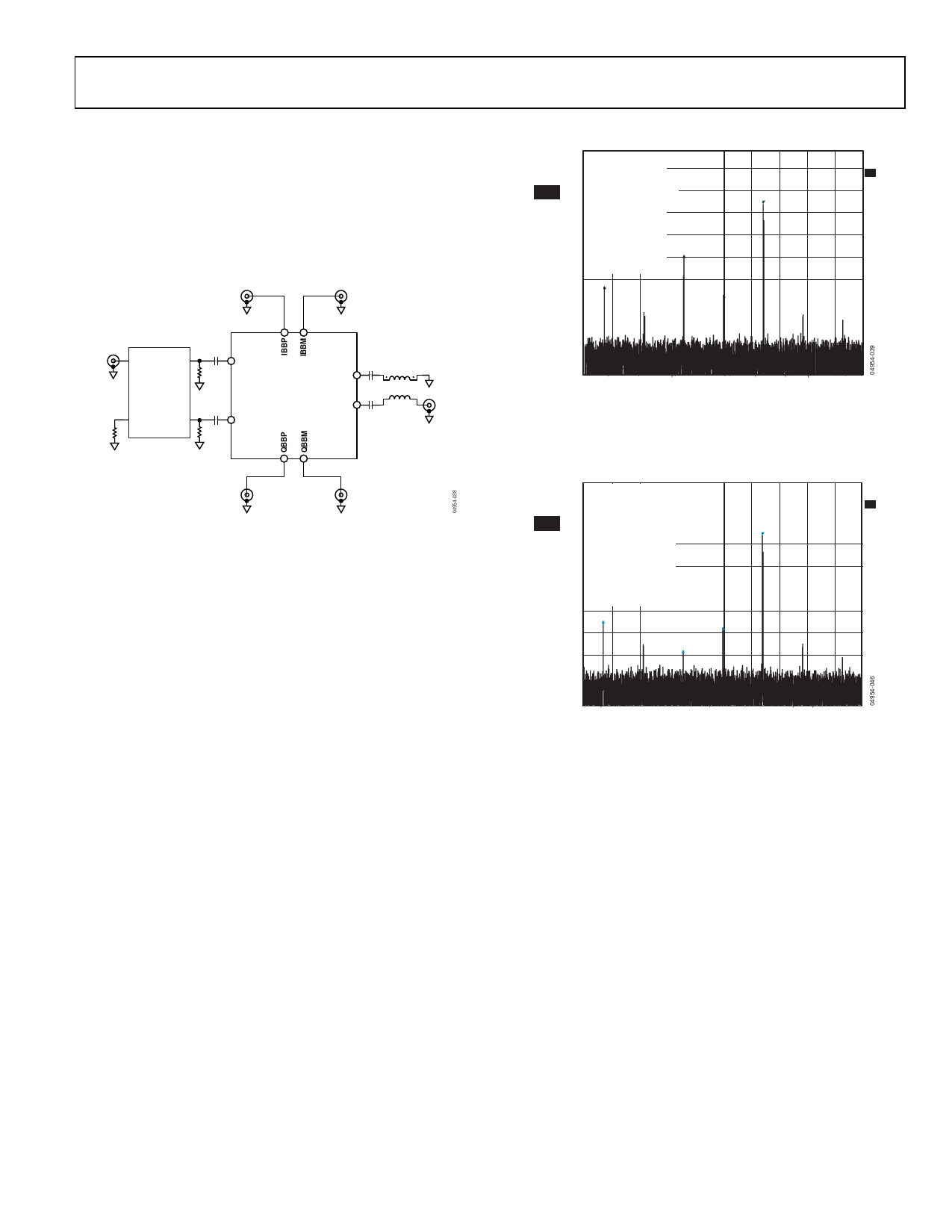
Single sideband performance of a quadrature modulator is
determined by the magnitude and phase balance (compared to
a 90o offset) at the summation point of the I and Q signals.
Because the ADL5390 has matched amplifiers and mixers in
the I and Q channel, most of the single sideband performance
will be determined by the external 90o phase splitter. Good
single sideband performance can be achieved by choosing a
well-balanced 90o phase splitter. However, phase and magnitude
differences in the 90o phase splitter can be corrected by adjusting
the magnitude and phase of the I and Q data. Figure 39 shows
the performance of the ADL5390 used in conjunction with Mini-
Circuits QCN-12 90o power splitter. Figure 40 shows the single
sideband improvement as the I and Q data is adjusted in magnitude
and phase to achieve better single sideband performance.
For maximum dynamic range, the ADL5390 should be driven
as close to the output 1 dB compression point as possible. The
output power of the ADL5390 increases linearly with the RF
(LO) input power and baseband gain control input voltage until
the ADL5390 reaches compression. At the 1 dB compression
point, the lower sideband starts to increase. Figure 41 demon-
strates the output spectrum of a 3-carrier CDMA2000 signal
applied to the I/Q baseband gain control inputs. As the RF (LO)
power is increased, the relative amount of noise is reduced until
the ADL5390 goes into compression. At this point, the relative
noise increases, as shown in Figure 42.
Analog Devices has several quadrature/vector modulators that
have highly accurate integrated 90o phase splitters—AD8340,
AD8341, AD8345, AD8346, AD8349—that cover a variety of
frequency bands.
ADL5390
REF 7dBm
ATT 35dB
* RBW 3kHz
VWB 10kHz
SWT 780ms
DESIRED SIDEBAND
0 –16.20dBm
900.998397436MHz
A
1 AP
CLRWR
–10
UNDESIRED SIDEBAND
–23.27dB
1
–20 –1.996794872MHz
THIRD BASEBAND HARMONIC
–30
–37.38dB
–4.004807692MHz
LO FEEDTHROUGH
2
–40 –41.27dB
–998.397435897kHz
–50
3
4
–60
–70
-80
-90
CENTER 900MHz
700kHz/
SPAN 7MHz
Figure 39. SSB Quadrature Modulator Result Using External 90° Phase Splitter,
RF PIN = −15 dBm, VIBB = VQBB = 0.5 V
(With Reference to a Common-Mode Voltage of 0.5 V)
REF 7dBm
ATT 35dB
* RBW 3kHz
VWB 10kHz
SWT 780ms
DESIRED SIDEBAND
0 –16.78dBm
A
900.998397436MHz
1 AP
CLRWR
–10
UNDESIRED SIDEBAND
–51.81dB
1
–20 –1.996794872MHz
THIRD BASEBAND HARMONIC
–30
–38.45dB
–4.004807692MHz
LO FEEDTHROUGH
–40 –41.49dB
–998.397435897kHz
–50 3
4
–60
2
–70
–80
–90
CENTER 900MHz
700kHz/
SPAN 7MHz
Figure 40. SSB Modulator Applications with Gain and Phase Errors Corrected,
RF Pin = −15 dBm, VIBB = VQBB = 0.5 V (With Reference to a Common-Mode
Voltage of 0.5 V), I/Q Phase Offset by 3o, and Magnitude Offset by 0.5 V
Rev. 0 | Page 17 of 24
Share Link: 