BT869KRF Ver la hoja de datos (PDF) - Conexant Systems
Número de pieza
componentes Descripción
Lista de partido
BT869KRF Datasheet PDF : 104 Pages
| |||
1.0 Functional Description
1.1 Pin Descriptions
Bt868/Bt869
Flicker-Free Video Encoder with UltrascaleTM Technology
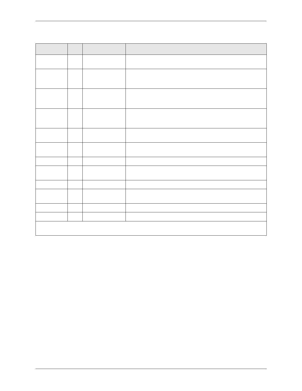
Table 1-1. Pin Assignments (3 of 3)
Pin Name I/O
Pin #
Description
FSADJUST
VBIAS
I 78
O 77
VREF
O 76
COMP
O 75
AGND_DAC
VAA_DACC
DACC
VAA_DACB
DACB
VAA_DACA
DACA
N/C
— 74
— 73
O 72
— 71
O 70
— 69
O 68
— 65, 66, 67
Full-scale adjust control pin. A resistor (RSET) connected between this pin
and GND controls the full-scale output current on the analog outputs.
DAC bias voltage. A 0.1 µF ceramic capacitor must be used to bypass this
pin to GND. The capacitor must be as close to the device as possible to keep
lead lengths to an absolute minimum.
Voltage reference pin. A 0.1 µF ceramic capacitor must be used to decouple
this pin to GND. The decoupling capacitor must be as close to the device as
possible to keep lead lengths to an absolute minimum.
Compensation pin. A 0.1 µF ceramic capacitor must be used to bypass this
pin to VAA. The capacitor must be as close to the device as possible to keep
lead lengths to an absolute minimum.
Common DAC Analog ground return. All AGND and VSS pins must be
connected together on the same PCB plane to prevent latchup.
DACC Analog power. All VAA and VDD pins must be connected together on
the same PCB plane to prevent latchup.
DACC output.
DACB Analog power. All VAA and VDD pins must be connected together on
the same PCB plane to prevent latchup.
DACB output.
DACA Analog power. All VAA and VDD pins must be connected together on
the same PCB plane to prevent latchup.
DACA output.
No connect pins
NOTE(S):
(1) Any unused inputs should not be left floating.
1-4
Conexant
100123B
Share Link: 