WSE128K16-35G2TC Ver la hoja de datos (PDF) - Unspecified
Número de pieza
componentes Descripción
Lista de partido
WSE128K16-35G2TC Datasheet PDF : 15 Pages
| |||
WSE128K16-XXX
EEPROM WRITE
A write cycle is initiated when OE is high and a low pulse is on
EWE or ECS with ECS or EWE low. The address is latched on the
falling edge of ECS or EWE whichever occurs last. The data is
latched by the rising edge of ECS or EWE, whichever occurs first.
A byte write operation will automatically continue to completion.
WRITE CYCLE TIMING
Figures 7 and 8 show the write cycle timing relationships. A
write cycle begins with address application, write enable and
chip select. Chip select is accomplished by placing the ECS
line low. Write enable consists of setting the EWE line low.
The write cycle begins when the last of either ECS or EWE goes
low.
The EWE line transition from high to low also initiates an
internal 150 µsec delay timer to permit page mode operation.
Each subsequent EWE transition from high to low that occurs
before the completion of the 150 µsec time out will restart the
timer from zero. The operation of the timer is the same as a
retriggerable one-shot.
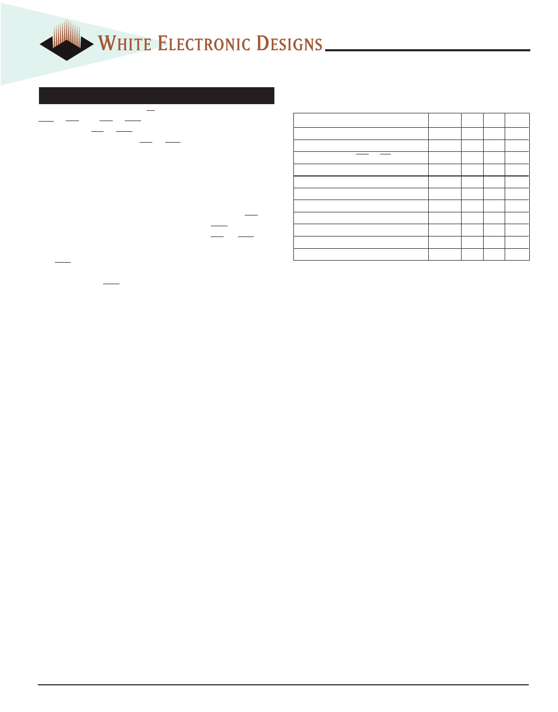
EEPROM AC WRITE CHARACTERISTICS
(VCC = 5.0V, VSS = 0V, TA = -55°C to +125°C)
Write Cycle Parameter
Write Cycle Time, TYP = 6ms
Address Set-up Time
Write Pulse Width (EWE or ECS)
Chip Select Set-up Time
Address Hold Time
Data Hold Time
Chip Select Hold Time
Data Set-up Time
Output Enable Set-up Time
Output Enable Hold Time
Write Pulse Width High
Symbol Min
tWC
tAS
0
tWP 150
tCS
0
tAH 100
tDH
10
tCSH
0
tDS 100
tOES
10
tOEH
10
tWPH
50
Max Unit
10 ms
ns
ns
ns
ns
ns
ns
ns
ns
ns
ns
White Electronic Designs Corporation • Phoenix, AZ • (602) 437-1520
6
Share Link: 