SMS24 Ver la hoja de datos (PDF) - Summit Microelectronics
Número de pieza
componentes Descripción
Lista de partido
SMS24 Datasheet PDF : 18 Pages
| |||
SMS24
DEVICE OPERATION
REGISTERS
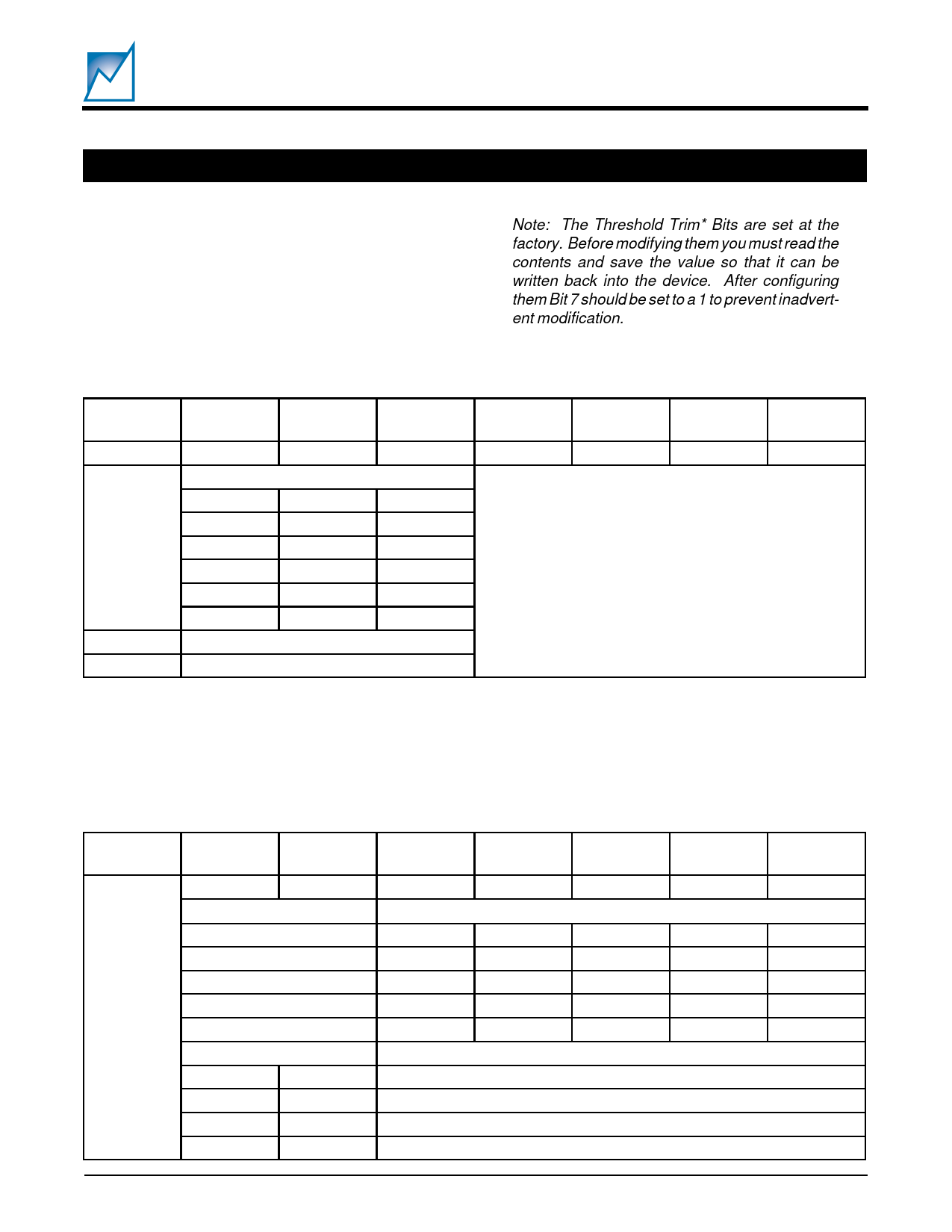
Configuration Register
The configuration Register, located at address 00, is
illustrated in Table 1. The Configuration Bits (6, 5, & 4)
select the basic Device Code, and are referred to as Con2,
Con1, and Con0. Bit 7 is the Lock Bit, and when set to 1
locks the contents of the register.
Note: The Threshold Trim* Bits are set at the
factory. Before modifying them you must read the
contents and save the value so that it can be
written back into the device. After configuring
them Bit 7 should be set to a 1 to prevent inadvert-
ent modification.
Table 1. Configuration Register
MSB
7
6
5
4
3
LOCK
Con2
Con1
Con0
T3
Valid Device Codes
0
0
1
0
1
0
x
0
1
1
1
0
0
1
0
1
1
1
0
0
Configuration Register Open
1
Configuration Locked (non-volatile)
Programming Registers
Once the device has been configured it is a simple matter
of writing to the two Programming Registers to prepare the
device for operation.
2
1
T2
T1
Threshold Trim *
LSB
0
T0
2046 Table01 2.0
Table 2. Programming Register 0
MSB
7
x
6
5
4
3
2
1
RT1
RT0
RR4
RR3
RR2
RR1
Reset Threshold Volts
Reset Threshold Bits
2.15V à
0
0
0
0
2.65V à
0
0
0
1
2.90V à
0
0
1
0
4.375V à
0
1
0
0
4.625V à
1
0
0
0
Reset Timeout Bits Reset Timeout Seconds
0
0
ß 25ms
0
1
ß 50ms
1
0
ß 100ms
1
1
ß 200ms
SUMMIT MICROELECTRONICS, Inc.
2048 2.4. 3/1/01
LSB
0
RR0
1
0
0
0
0
2046 Table02 2.0
7
Share Link: 