ML2721 Ver la hoja de datos (PDF) - Micro Linear Corporation
Número de pieza
componentes Descripción
Lista de partido
ML2721 Datasheet PDF : 27 Pages
| |||
PRELIMINARY
MODES OF OPERATION (CONTINUED)
ILO
DATA FILTER
QLO
F
V
∫
ML2721
FREF or
FREF/2
CAL I
TONE
GEN
Q
FCOMP
TRACKING
COUNTER
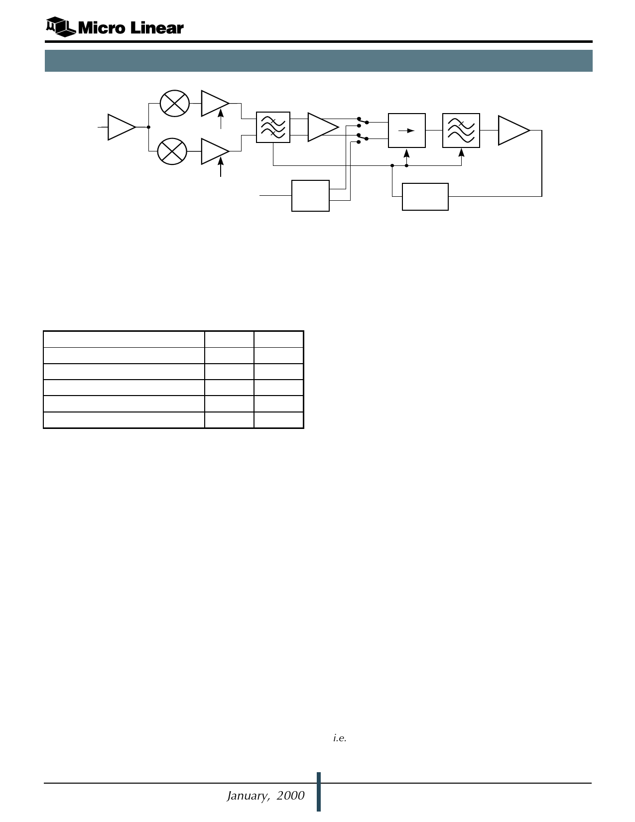
Figure 2. Dual Modulus Signal Divider
The signal flow in RECEIVE mode is from the RF input,
through an image reject mixer, IF filter, hard limiter,
Frequency to Voltage converter, data filter and data slicer.
The ML2721 uses a single conversion super heterodyne
receiver with a nominal IF of 1.024 MHz. An AGC
subsystem extends the dynamic range of the receiver. The
IF frequency and filter bandwidths are given in Table 3.
Reference Division Ratio
6
12
Parameter
RD0 = 0 RD0 = 1
IF filter center frequency
REF/6 REF/12
IF filter bandwidth
REF/4.4 REF/8.8
Receive data filter
REF/8 REF/16
F to V converter center frequency REF/6 REF/12
Table 3. Filter Parameters to Division Ratio
Major features of the receiver are:
n High dynamic range mixers with 10dB noise figure, –
15dBm IP3, 35dB image rejection (typical)
n 6-pole bandpass IF filter, with accurate Gaussian to
12dB response
n Center frequency 1.024MHz, Bandwidth 1.408 MHz
(nominal)
n Limiting IF amplifiers with >80dB gain, and excellent
AM rejection
n AGC to extend the dynamic range of the integrated
filters & RSSI
n Logarithmic RSSI output from Limiter; AGC state is
information added to give 80dB range
n FM demodulation by a linear F-to-V converter
n 5-pole low-pass data filter with an accurate Gaussian
response and 3dB cutoff at 768kHz (nominal)
n 2 level data slicer with DC offset removal
The output of the receiver is quantized in amplitude (to 1
bit) but there is no internal timing recovery. Timing
recovery is performed in the external baseband circuits.
FILTER ALIGNMENT
In RXCAL mode the receiver is not functional. Instead, the
ML2721 filter alignment function tunes all the internal
filters using the reference frequency from the REF pin. See
Figure 2.
The IF filter, data filters, and the F-to-V converter all have
their frequency responses governed by RC time constants.
Every capacitor that affects the frequency response
includes a binary weighted capacitor array controlled by
a 7 bit tuning bus. In RXCAL mode a reference tone at the
IF center frequency is routed to the F-to-V converter. A
digital tracking loop then adjusts the tuning word until
there is mid-rail output from the F-to-V converter. This
tracking loop may take up to 300µs to tune the filter when
XCEN is asserted, but the tracking loop will continue to
make small adjustments whenever the ML2721 is in
RXCAL mode. Because all the filters in the chip are tuned
in this manner, centering the F-to-V converter sets up the
correct center frequencies and bandwidths for all the
filters.
The ML2721 must be placed in RXCAL mode for 300µs
whenever XCEN is asserted to give time for the filters to
align completely.
Data Slicer
The data slicer is a comparator that is AC coupled to the
receive data filter output. The output is logic high or logic
low. This circuit is designed to rapidly acquire valid data
at the beginning of a received packet of data. The
nominal time constant for the AC coupling is 9µs. This
limits the maximum recommended run length to four ones
or zeroes at 1.3Mbps. Longer run lengths require the use
of a more complex external data slicer circuit.
Data Output Drive
The ML2721 DOUT pin is designed to drive a PCB trace
and a single logic input with controlled slew rates. Buffer
the output when driving any logic load greater than 5pF
(i.e., more than an ´10 oscilloscope probe or a single
CMOS logic input pin).
January, 2000 PRELIMINARY DATASHEET
11
Share Link: 