P4C1981-10JC Ver la hoja de datos (PDF) - Performance Semiconductor
Número de pieza
componentes Descripción
Lista de partido
P4C1981-10JC Datasheet PDF : 10 Pages
| |||
P4C1981/1981L, P4C1982/1982L
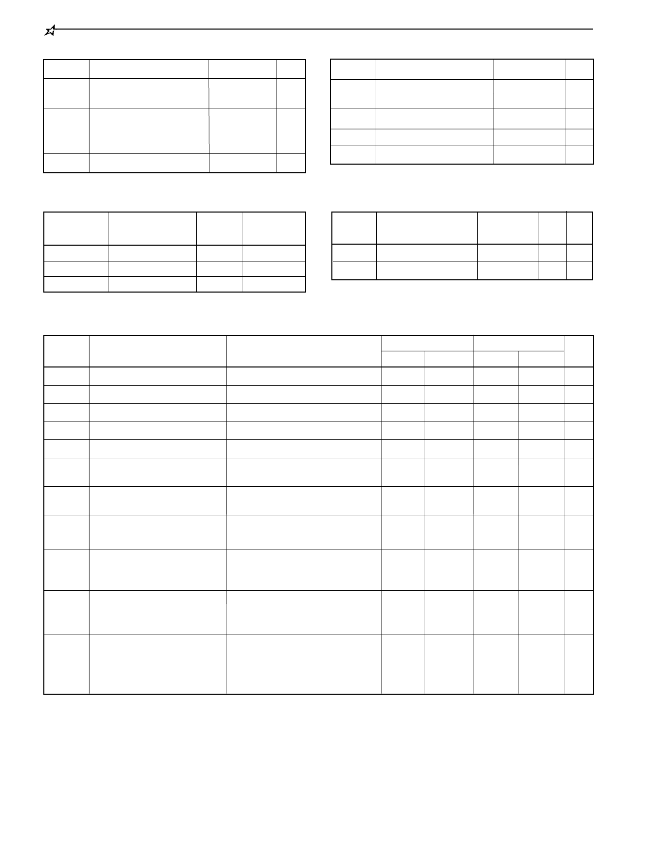
MAXIMUM RATINGS(1)
Symbol
Parameter
VCC
Power Supply Pin with
Respect to GND
V
TERM
Terminal Voltage with
Respect to GND
(up to 7.0V)
TA
Operating Temperature
Value Unit
–0.5 to +7 V
–0.5 to
V +0.5 V
CC
–55 to +125 °C
RECOMMENDED OPERATING
TEMPERATURE AND SUPPLY VOLTAGE
Grade(2)
Ambient
Temperature
Military
–55°C to +125°C
Industrial –40°C to +85°C
Commercial 0°C to +70°C
GND
0V
0V
0V
VCC
5.0V ± 10%
5.0V ± 10%
5.0V ± 10%
Symbol Parameter
T
BIAS
Temperature Under
Bias
TSTG
Storage Temperature
PT
Power Dissipation
IOUT
DC Output Current
Value Unit
–55 to +125 °C
–65 to +150 °C
1.0
W
50
mA
CAPACITANCES(4)
VCC = 5.0V, TA = 25°C, f = 1.0MHz
Symbol
Parameter
Conditions Typ. Unit
CIN
COUT
Input Capacitance VIN = 0V 5 pF
Output Capacitance VOUT = 0V 7 pF
DC ELECTRICAL CHARACTERISTICS
Over recommended operating temperature and supply voltage(2)
Symbol
Parameter
Test Conditions
P4C1981 / 1982 P4C1981L / 82L Unit
Min Max
Min
Max
VIH
Input High Voltage
VIL
Input Low Voltage
VHC
CMOS Input High Voltage
VLC
CMOS Input Low Voltage
2.2 VCC +0.5 2.2 VCC +0.5 V
–0.5(3)
0.8
–0.5(3)
0.8
V
VCC –0.2 VCC +0.5 VCC –0.2 VCC +0.5 V
–0.5(3)
0.2
–0.5(3)
0.2
V
VCD
Input Clamp Diode Voltage VCC = Min., IIN = –18 mA
VOL
Output Low Voltage
(TTL Load)
IOL = +8 mA, VCC = Min.
–1.2
–1.2 V
0.4
0.4 V
VOH
Output High Voltage
IOH = –4 mA, VCC = Min.
2.4
(TTL Load)
2.4
V
ILI
Input Leakage Current
VCC = Max.
Mil. –10
+10
–5
+5 µA
VIN = GND to VCC
Com’l. –5
+5
n/a
n/a
ILO
Output Leakage Current VCC = Max.,
Mil. –10
+10
–5
+5 µA
CE , CE = V
1
2
IH
Ind./Com’l. –5
+5
n/a
n/a
VOUT = GND to VCC
ISB
Standby Power Supply
CE1,
CE
2
≥
VIH,
Current (TTL Input Levels) VCC = Max.,
Mil. ___
Ind./Com’l. ___
40
35
___
40 mA
___
n/a
f = Max., Outputs Open
ISB1
Standby Power Supply
Current
CE1,
CE
2
≥
VHC,
VCC = Max.,
Mil. ___
Ind./Com’l. ___
20
15
___
1.0 mA
___
n/a
(CMOS Input Levels)
f = 0, Outputs Open
V
IN
≤
V
LC
or
V
IN
≥
V
HC
n/a = Not Applicable
Notes:
1. Stresses greater than those listed under MAXIMUM RATINGS may
cause permanent damage to the device. This is a stress rating only
and functional operation of the device at these or any other conditions
above those indicated in the operational sections of this specification
is not implied. Exposure to MAXIMUM ratingconditions for extended
periods may affect reliability.
2. Extended temperature operation guaranteed with 400 linear feet per
minute of air flow.
3. Transient inputs with VIL and IIL not more negative than –3.0V and
–100mA, respectively, are permissible for pulse widths up to 20 ns.
4. This parameter is sampled and not 100% tested.
82
Share Link: 