IC555 Ver la hoja de datos (PDF) - Fairchild Semiconductor
Número de pieza
componentes Descripción
Lista de partido
IC555 Datasheet PDF : 14 Pages
| |||
Application Information
Table 1 below is the basic operating table of 555 timer.
Table 1. Basic Operating Table
Reset
(PIN 4)
VTR
(PIN 2)
VTH
(PIN 6)
Output
(PIN 3)
Discharging
Transistor
(PIN 7)
Low
X
X
Low
ON
High
< 1/3 VCC
X
High
OFF
High
> 1/3 VCC
> 2/3 VCC
Low
ON
High
> 1/3 VCC
< 2/3 VCC
Previous State
When the low signal input is applied to the reset terminal, the timer output remains low regardless of the threshold volt-
age or the trigger voltage. Only when the high signal is applied to the reset terminal, the timer's output changes accord-
ing to threshold voltage and trigger voltage.
When the threshold voltage exceeds 2/3 of the supply voltage while the timer output is high, the timer's internal dis-
charge transistor turns on, lowering the threshold voltage to below 1/3 of the supply voltage. During this time, the timer
output is maintained low. Later, if a low signal is applied to the trigger voltage so that it becomes 1/3 of the supply volt-
age, the timer's internal discharge transistor turns off, increasing the threshold voltage and driving the timer output
again at high.
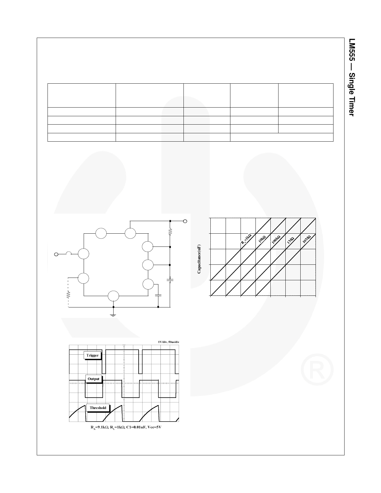
1. Monostable Operation
Trigger
RL
4
RESET
2 TRIG
8
Vcc
DISCH 7
THRES 6
3 OUT
GND
1
CONT 5
+Vcc
RA
C1
C2
102
101
=1kΩ
RA
10kΩ
100kΩ
1MΩ
Ω
10M
100
10-1
10-2
10-3
10-5
10-4
10-3
10-2
10-1
100
101
102
Time Delay(s)
Figure2. Monostable Circuit
Figure 3. Resistance and Capacitance vs.
Time Delay (tD)
Figure 4. Waveforms of Monostable Operation
© 2002 Fairchild Semiconductor Corporation
LM555 Rev. 1.1.0
4
www.fairchildsemi.com
Share Link: 