IC555 Ver la hoja de datos (PDF) - Fairchild Semiconductor
Número de pieza
componentes Descripción
Lista de partido
IC555 Datasheet PDF : 14 Pages
| |||
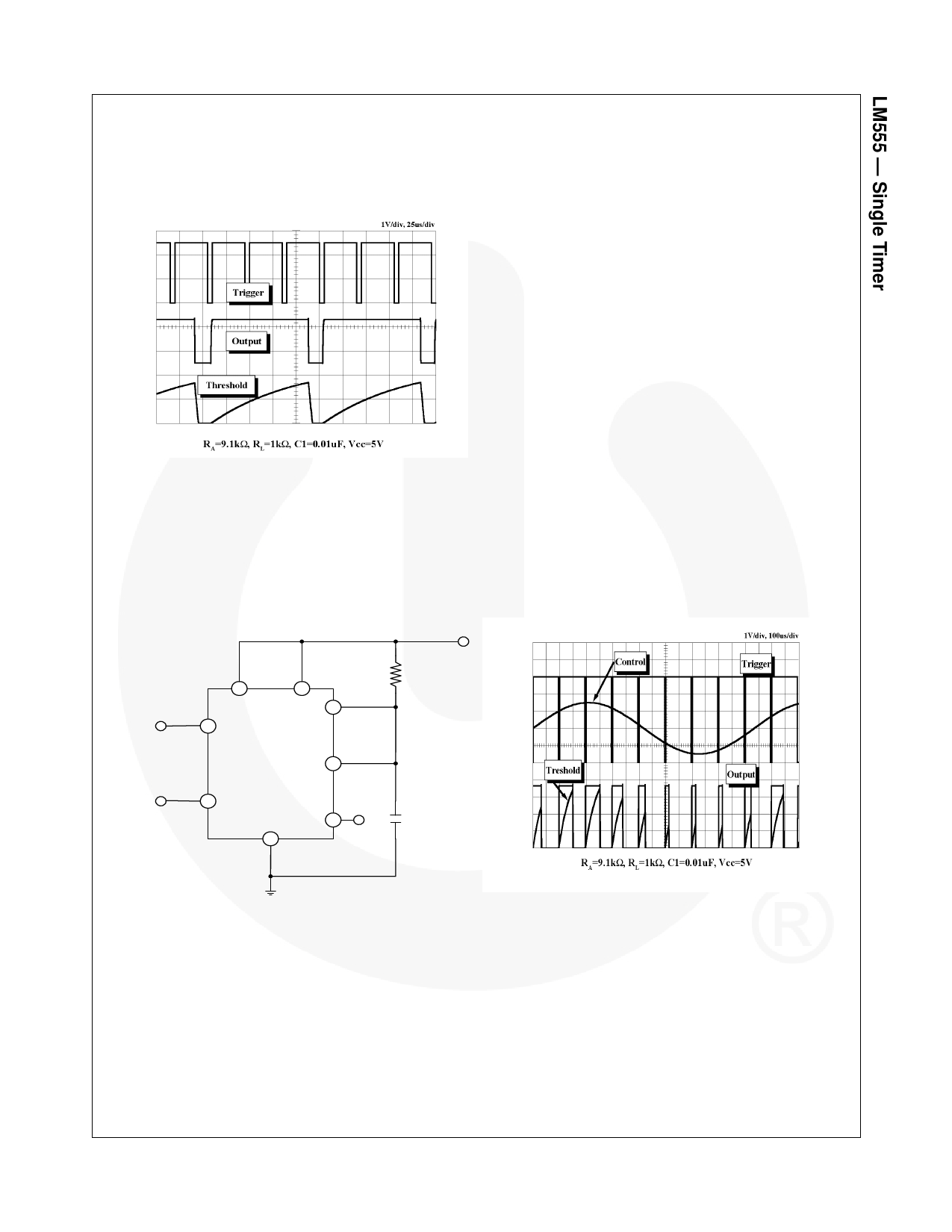
3. Frequency Divider
By adjusting the length of the timing cycle, the basic circuit of Figure 1 can be made to operate as a frequency divider.
Figure 9. illustrates a divide-by-three circuit that makes use of the fact that retriggering cannot occur during the timing
cycle.
Figure 9. Waveforms of Frequency Divider Operation
4. Pulse Width Modulation
The timer output waveform may be changed by modulating the control voltage applied to the timer's pin 5 and chang-
ing the reference of the timer's internal comparators. Figure 10 illustrates the pulse width modulation circuit.
When the continuous trigger pulse train is applied in the monostable mode, the timer output width is modulated accord-
ing to the signal applied to the control terminal. Sine wave, as well as other waveforms, may be applied as a signal to
the control terminal. Figure 11 shows the example of pulse width modulation waveform.
+Vcc
RA
4
8
Trigger
RESET
2 TRIG
Vcc
7
DISCH
6
Output
3 OUT
THRES
Input
GND
CONT 5
C
1
Figure 10. Circuit for Pulse Width Modulation
Figure 11. Waveforms of Pulse Width Modulation
© 2002 Fairchild Semiconductor Corporation
LM555 Rev. 1.1.0
8
www.fairchildsemi.com
Share Link: 