LPC47N227-MN Ver la hoja de datos (PDF) - SMSC -> Microchip
Número de pieza
componentes Descripción
Lista de partido
LPC47N227-MN Datasheet PDF : 202 Pages
| |||
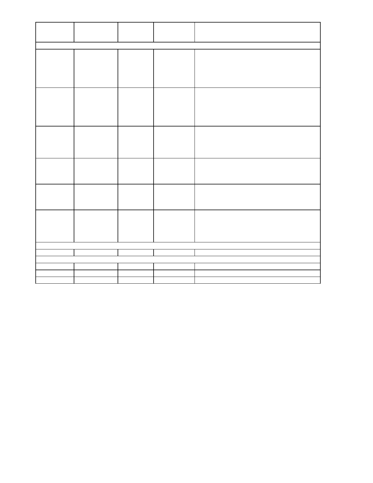
TQFP/STQFP
PIN #
6,
32-39, 40-47
48,
54-56,
57-59
49
50
51
52
64
19
53,65,93
18
7,31, 60,76
NAME
General
Purpose I/O
(Note 9)
General
Purpose I/O
(System Option)
(Note 5)
(Note 9)
General
Purpose I/O/
System Mgt.
Interrupt
(Note 9)
General
Purpose I/O/
IRQ Input 1
(Note 9)
General
Purpose I/O/
IRQ Input 2
(Note 9)
General
Purpose I/O/
Floppy on
Parallel Port
(Note 9)
14MHz Clock
VCC (Note 6)
VTR (Note 6)
VSS
BUFFER
SYMBOL
TYPE PER
FUNCTION1
DESCRIPTION
GENERAL PURPOSE I/O
GP24,
(I/O8/OD8) Dedicated General Purpose Input/Output.
GP30-GP37
GP40-GP47
GP10,
GP15-GP17,
GP20-GP22
GP11/
(I/O8/OD8) General Purpose Input/Output.
(SYSOPT)
GP12/
(I/O12/OD12)/
At the trailing edge of hardware reset the GP11 pin
is latched to determine the configuration base
address: 0 = Index Base I/O Address 02E Hex; 1 =
Index Base I/O Address 04E Hex.
General Purpose Input/Output.
nIO_SMI
(O12/OD12) Active low System Management Interrupt Output.
GP13/
IRQIN1
GP14/
IRQIN2
GP23/
FDC_PP
(I/O8/OD8)/ General Purpose Input/Output.
I
(I/O8/OD8)/
External Interrupt Input. Steerable onto one of the
15 Serial IRQs.
General Purpose Input/Output.
I
(I/O8/OD8)/
External Interrupt Input. Steerable onto one of the
15 Serial IRQs.
General Purpose Input/Output.
I
Floppy on the Parallel Port Indication.
CLOCKI
VCC
VTR
VSS
CLOCK PINS
IS
14.318MHz Clock Input.
POWER PINS
+3.3 Volt Supply Voltage.
+3.3 Volt Standby Voltage.
Ground.
Note: The "n" as the first letter of a symbol indicates an "Active Low" signal.
Note 1: Buffer types per function on multiplexed pins are separated by a slash “/”. Buffer types in
parenthesis represent multiple buffer types for a single pin function.
Note 2: The nLPCPD pin may be tied high.
Note 3: The FDD output pins multiplexed in the PARALLEL PORT INTERFACE are OD drivers only and
are not affected by the FDD Output Driver Controls (see subsection CR05 in the Configuration
section).
Note 4: Active (push-pull) output drivers are required on these pins in the enhanced parallel port modes.
11
Share Link: 