SC18IM700 Ver la hoja de datos (PDF) - NXP Semiconductors.
Número de pieza
componentes Descripción
Lista de partido
SC18IM700 Datasheet PDF : 24 Pages
| |||
NXP Semiconductors
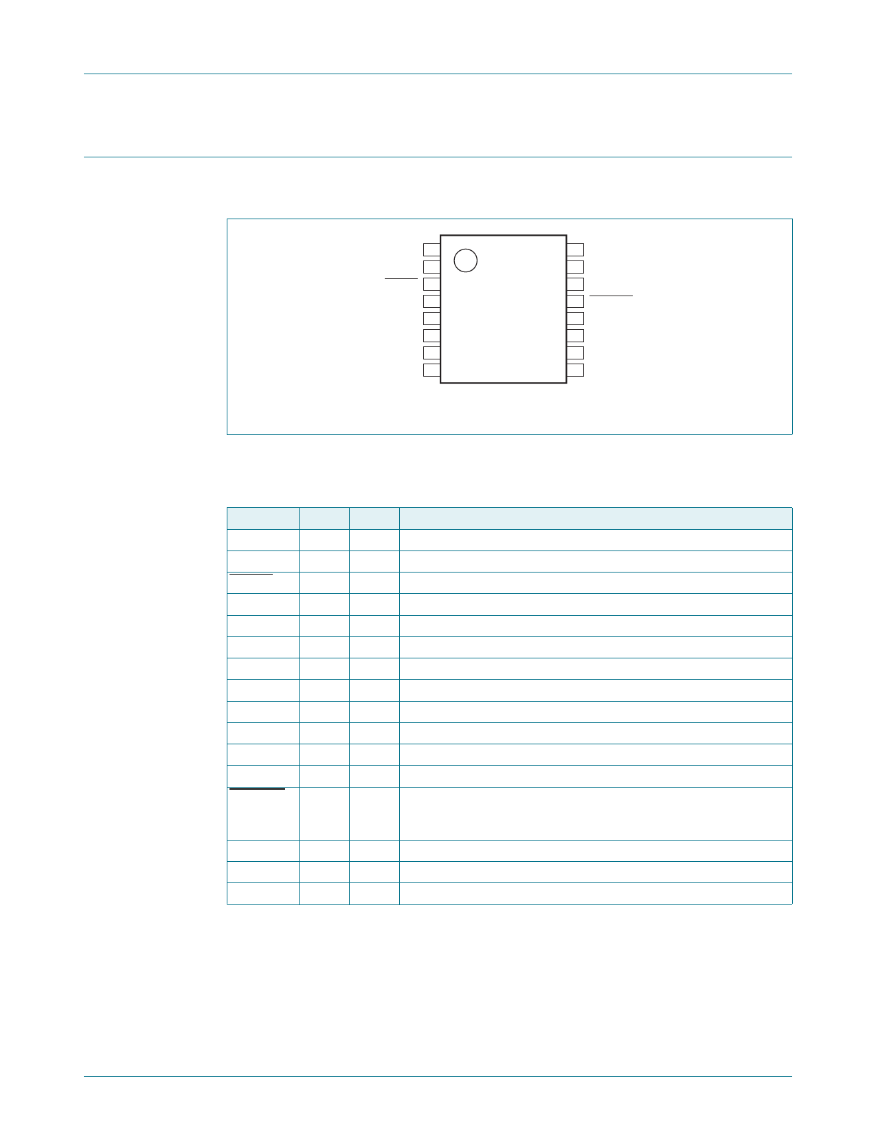
6. Pinning information
6.1 Pinning
SC18IM700
Master I2C-bus controller with UART interface
GPIO0 1
GPIO1 2
RESET 3
VSS 4
GPIO2 5
GPIO3 6
SDA 7
SCL 8
SC18IM700IPW
SC18IM700IPW/S8
16 GPIO7
15 GPIO4
14 GPIO5
13 WAKEUP
12 VDD
11 GPIO6
10 TX
9 RX
002aab798
Fig 2. Pin configuration for TSSOP16
6.2 Pin description
Table 3. Pin description
Symbol Pin Type Description
GPIO0 1
I/O programmable I/O pin
GPIO1 2
I/O programmable I/O pin
RESET 3
I
hardware reset input
VSS
4
GPIO2 5
-
ground
I/O programmable I/O pin
GPIO3 6
I/O programmable I/O pin
SDA
7
I/O
I2C-bus data pin
SCL
8
O
I2C-bus clock output
RX
9
I
RS-232 receive input
TX
10
O
RS-232 transmit input
GPIO6 11
I/O programmable I/O pin
VDD
12
WAKEUP 13
GPIO5 14
-
power supply
I
Wake up SC18IM700 from Power-down mode. Pulling LOW by the
host to wake up the device. A 1 k resistor must be connected
between VDD and this pin.
I/O programmable I/O pin
GPIO4 15
O
programmable I/O pin
GPIO7 16
O
programmable I/O pin
SC18IM700_3
Product data sheet
All information provided in this document is subject to legal disclaimers.
Rev. 3 — 12 October 2017
© NXP Semiconductors N.V. 2017. All rights reserved.
3 of 24
Share Link: 