HIP6020 Ver la hoja de datos (PDF) - Intersil
Número de pieza
componentes Descripción
Lista de partido
HIP6020 Datasheet PDF : 15 Pages
| |||
HIP6020
Electrical Specifications Recommended Operating Conditions, Unless Otherwise Noted. Refer to Figures 1, 2 and 3 (Continued)
PARAMETER
SYMBOL
TEST CONDITIONS
MIN TYP MAX UNITS
PWM CONTROLLERS GATE DRIVERS
UGATE1,2 Source
UGATE1,2 Sink
LGATE Source
LGATE Sink
PROTECTION
IUGATE
RUGATE
ILGATE
RLGATE
VCC = 12V, VUGATE1 (or VUGATE2) = 6V
VGATE-PHASE = 1V
VCC = 12V, VLGATE1 = 1V
VLGATE = 1V
-
1
-
A
-
1.7 3.5
Ω
-
1
-
A
-
1.4 3.0
Ω
VSEN1 Over-Voltage (VSEN1/DACOUT)
VSEN1 Rising
-
115 120
%
FAULT Sourcing Current
OCSET1,2 Current Source
Soft-Start Current
POWER GOOD
IOVP
IOCSET
ISS
VFAULT/RT = 2.0V
VOCSET = 4.5VDC
-
8.5
-
mA
170 200 230
µA
-
28
-
µA
VSEN1 Upper Threshold
(VSEN1/DACOUT)
VSEN1 Rising
108
-
110
%
VSEN1 Under-Voltage
(VSEN1/DACOUT)
VSEN1 Rising
92
-
94
%
VSEN1 Hysteresis (VSEN1/DACOUT)
Upper/Lower Threshold
-
2
-
%
PGOOD Voltage Low
VPGOOD IPGOOD = -4mA
-
-
0.8
V
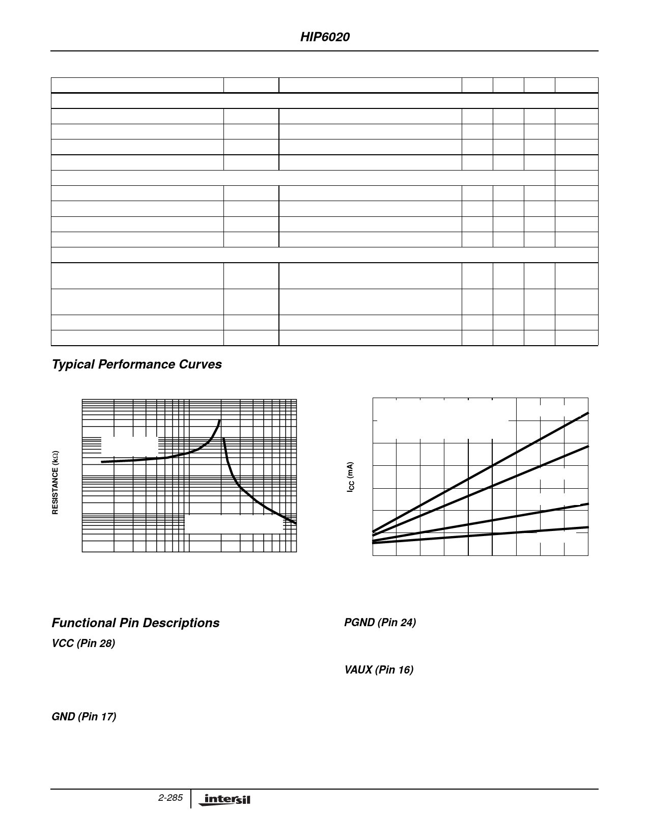
Typical Performance Curves
1000
100
RT PULLUP
TO +12V
10
RT PULLDOWN TO VSS
10
100
SWITCHING FREQUENCY (kHz)
1000
FIGURE 1. RT RESISTANCE vs FREQUENCY
Functional Pin Descriptions
VCC (Pin 28)
Provide a 12V bias supply for the IC to this pin. This pin also
provides the gate bias charge for all the MOSFETs
controlled by the IC. The voltage at this pin is monitored for
Power-On Reset (POR) purposes.
GND (Pin 17)
Signal ground for the IC. All voltage levels are measured with
respect to this pin.
140
CUGATE1 = CUGATE2 = CLGATE1 = C
120 VIN = 5V
VCC = 12V
100
C = 4800pF
80
C = 3600pF
60
C = 1500pF
40
20
C = 660pF
0
100 200 300 400 500 600 700 800 900 1000
SWITCHING FREQUENCY (kHz)
FIGURE 2. BIAS SUPPLY CURRENT vs FREQUENCY
PGND (Pin 24)
This is the power ground connection. Tie the synchronous
PWM converter’s lower MOSFET source to this pin.
VAUX (Pin 16)
The +3.3V input voltage at this pin is monitored for power-on
reset (POR) purposes. Connected to +5V input, this pin
provides boost current for the two linear regulator output
drives in the event bipolar NPN transistors (instead of
N-channel MOSFETs) are employed as pass elements.
2-285
Share Link: 