HIP6020 Ver la hoja de datos (PDF) - Intersil
Número de pieza
componentes Descripción
Lista de partido
HIP6020 Datasheet PDF : 15 Pages
| |||
HIP6020
Figure 7 shows a simplified schematic of the fault logic. An
over-voltage detected on VSEN1 immediately sets the fault
latch. A sequence of three over-current fault signals also
sets the fault latch. The over-current latch is set dependent
upon the states of the over-current (OC1 and OC2), linear
under-voltage (LUV) and the soft-start signals. A window
comparator monitors the SS pin and indicates when CSS is
fully charged to 4.5V (UP signal). An under-voltage on either
linear output (VSEN3 and VSEN4) is ignored until after the
soft-start interval (T4 in Figure 6). This allows VOUT3 and
VOUT4 to increase without fault at start-up. Cycling the bias
input voltage (+12VIN on the VCC pin off then on) resets the
counter and the fault latch.
Over-Voltage Protection
During operation, a short across the synchronous PWM
upper MOSFET (Q1) causes VOUT1 to increase. When the
output exceeds the over-voltage threshold of 115% of
DACOUT, the over-voltage comparator trips to set the fault
latch and turns the lower MOSFET (Q2) on. This blows the
input fuse and reduces VOUT1. The fault latch raises the
FAULT/RT pin to VCC.
A separate over-voltage circuit provides protection during
the initial application of power. For voltages on the VCC pin
below the power-on reset (and above ~4V), the output level
is monitored for voltages above 1.3V. Should VSEN1 exceed
this level, the lower MOSFET, Q2 is driven on.
Over-Current Protection
All outputs are protected against excessive over-currents.
Both PWM controllers use the upper MOSFET’s on-
resistance, rDS(ON) to monitor the current for protection
against shorted outputs. Both linear regulators monitor their
respective VSEN pins for under-voltage to protect against
excessive currents.
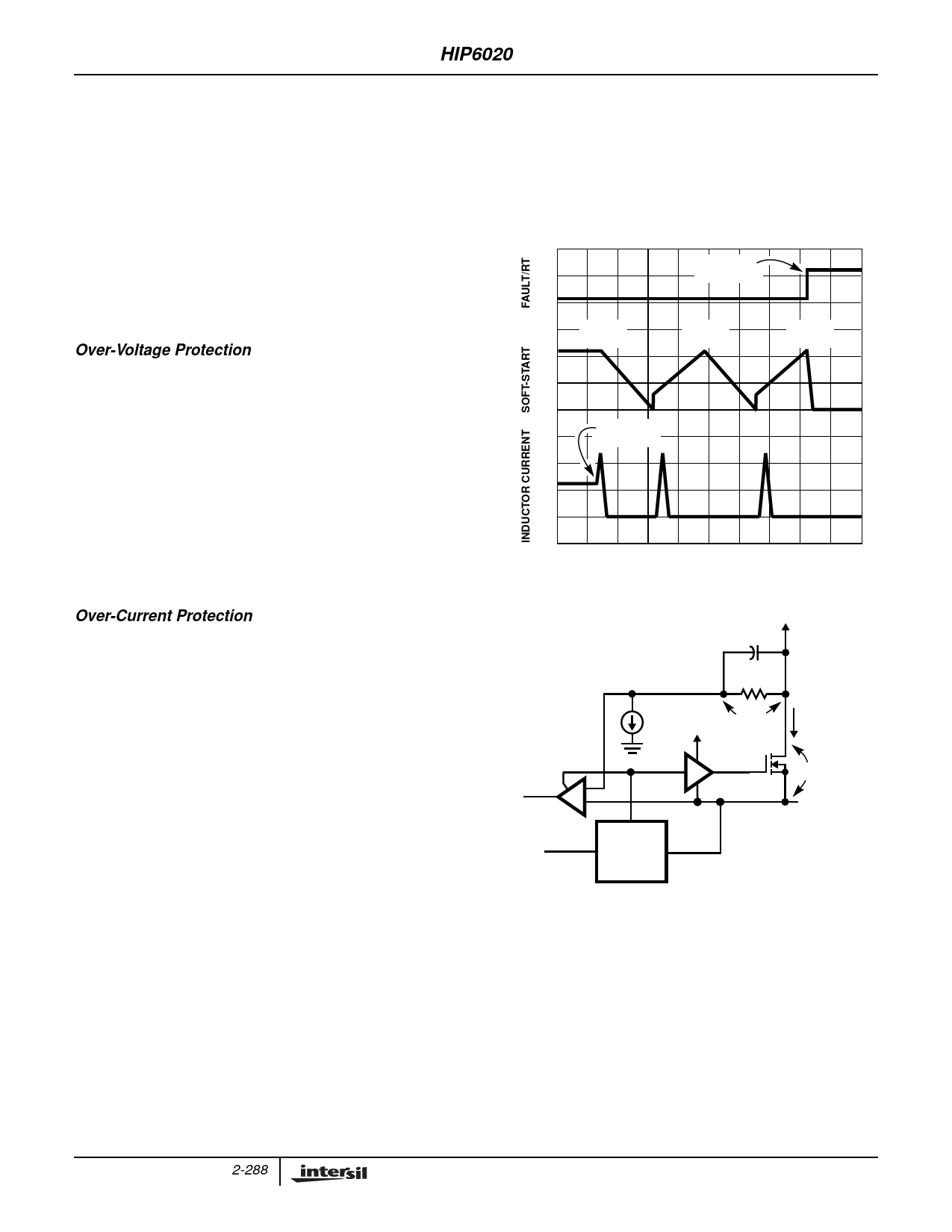
Figure 8 illustrates the over-current protection with an
overload on OUT2. The overload is applied at T0 and the
current increases through the inductor (LOUT2). At time T1,
the OVER-CURRENT2 comparator trips when the voltage
across Q3 (iD • rDS(ON)) exceeds the level programmed by
ROCSET. This inhibits all outputs, discharges the soft-start
capacitor (CSS) with a 28µA current sink, and increments the
counter. CSS recharges at T2 and initiates a soft-start cycle
with the error amplifiers clamped by soft-start. With OUT2 still
overloaded, the inductor current increases to trip the over-
current comparator. Again, this inhibits all outputs, but the
soft-start voltage continues increasing to 4.5V before
discharging. The counter increments to 2. The soft-start cycle
repeats at T3 and trips the over-current comparator. The SS
pin voltage increases to 4.5V at T4 and the counter
increments to 3. This sets the fault latch to disable the
converter. The fault is reported on the FAULT/RT pin.
The PWM1 controller operates in the same way as PWM2 to
over-current faults. Additionally, the two linear controllers
monitor the VSEN pins for an under-voltage. Should
excessive currents cause VSEN3 or VSEN4 to fall below the
linear under-voltage threshold, the LUV signal sets the over-
current latch, providing CSS is fully charged. Blanking the LUV
signal during the CSS charge interval allows the linear
outputs to build above the under-voltage threshold during
normal operation. Cycling the bias input power off then on
resets the counter and the fault latch.
FAULT
10V
REPORTED
0V
COUNT
=1
4V
COUNT
=2
COUNT
=3
2V
0V
OVERLOAD
APPLIED
0A
T0 T1
T2
TIME
T3
T4
FIGURE 5. OVER-CURRENT OPERATION
OVER-CURRENT TRIP:
VDS > VSET
iD × rDS(ON) > IOCSET × ROCSET
OCSET
VIN = +5V
ROCSET
OVER-
CURRENT
OC
+
-
IOCSET
200µA
DRIVE
VSET +
VCC
UGATE
PHASE
iD
+
VDS
PWM
GATE
CONTROL
VPHASE = VIN – VDS
VOCSET = VIN – VSET
FIGURE 6. OVER-CURRENT DETECTION
Resistors (ROCSET1 and ROCSET2) program the over-current
trip levels for each PWM converter. As shown in Figure 9, the
internal 200µA current sink (IOCSET) develops a voltage across
ROCSET (VSET) that is referenced to VIN. The DRIVE signal
enables the over-current comparator (OVER-CURRENT1 or
OVER-CURRENT2). When the voltage across the upper
MOSFET (VDS(ON)) exceeds VSET, the over-current
comparator trips to set the over-current latch. Both VSET and
VDS are referenced to VIN and a small capacitor across
ROCSET helps VOCSET track the variations of VIN due to
2-288
Share Link: 