78Q2120 Ver la hoja de datos (PDF) - TDK Corporation
Número de pieza
componentes Descripción
Lista de partido
78Q2120 Datasheet PDF : 33 Pages
| |||
78Q2120
10/100BASE-TX
Ethernet Transceiver
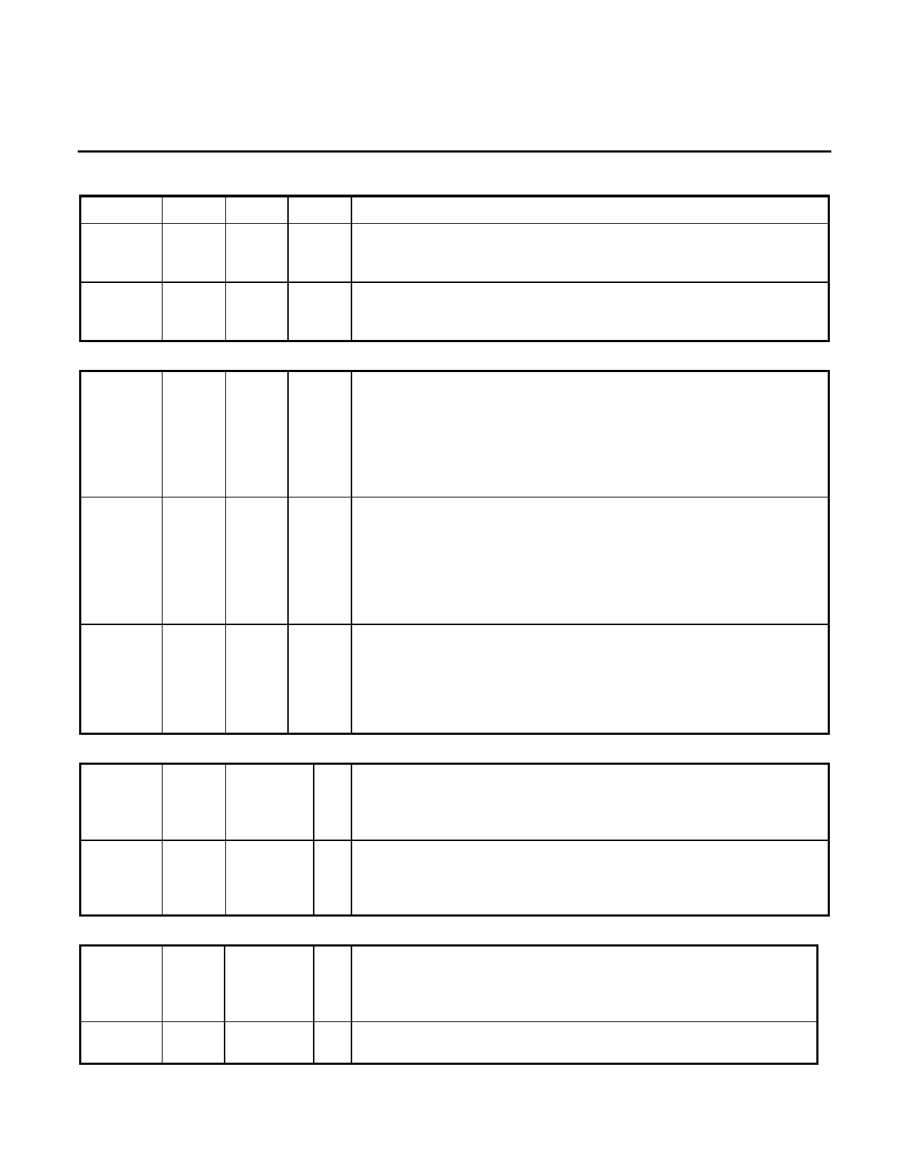
OSCILLATOR/CLOCK
NAME
CKIN
XTLP,
XTLN
64-PIN 80-PIN
4
5
59, 58 75,74
TYPE
I
A
DESCRIPTION
CLOCK INPUT: Connects to a 25 MHz clock source. This pin should
be held low when XTLP and XTLN are being used as the 25 MHz
clock source.
CRYSTAL PINS: Should be connected to a 25 MHz crystal. When
CKIN is being used as the 25 MHz clock source, these pins should be
connected together.
MISCELLANEOUS PINS
GPIO0
GPIO1
INTR
-
19
I/O GENERAL PURPOSE I/O PIN: This is an I/O pin which is
configurable as an input or an output via management interface. A
value of one in bit MR16.6 configures GPIO0 as an input, and a zero
configures it as an output. The logic level of the GPIO0 pin is reflected
in MR16.7. This pin has a weak internal pull-down to prevent it from
floating when configured as an input (it is configured as an input by
default).
-
20
I/O GENERAL PURPOSE I/O PIN: This is an I/O pin which is
configurable as an input or an output via the management interface. A
value of one in bit MR16.8 configures GPIO1 as an input, and a zero
configures it as an output. The logic level of the GPIO1 pin is reflected
in MR16.9. This pin has a weak internal pull-down to prevent it from
floating when configured as an input (it is configured as an input by
default).
35
43
OZ INTERRUPT PIN: This pin is used to signal an interrupt to the media
access controller. The pin is held in the high impedance state when
an interrupt is not indicated. The pin will be forced high or low to
signal an interrupt depending upon the value of the INTR_LEVEL bit
(MR16.14). The events which trigger an interrupt can be programmed
via the Interrupt Control Register located at address MR17.
POWER SUPPLY
VCC
GND
8, 11,
10,13,
S SUPPLY VOLTAGE: Two supply ranges are supported: 5V ± 0.5V, or
41, 43, 27,36, 49,
57, 63 52, 59, 60,
3.3V ± 0.3V.
73, 79 80
3, 5, 9, 4,7, 11,12, S GROUND
10, 42, 28, 35, 50,
53, 55, 51, 65, 71,
60
76
REFERENCE PIN
RIBB
56
RIBB_RET 54
72
A BIAS CURRENT SETTING RESISTOR: To be tied to an external
resistor which is also connected to pin 70. This resistor should be
placed as close as possible to the package pin. See Figure 1 for
suggested value.
70
A BIAS CURRENT SETTING RESISTOR RETURN PIN: To be
connected to external RIBB resistor.
9
Share Link: 