MTD800 Ver la hoja de datos (PDF) - Myson Century Inc
Número de pieza
componentes Descripción
Lista de partido
MTD800 Datasheet PDF : 42 Pages
| |||
MYSON
TECHNOLOGY
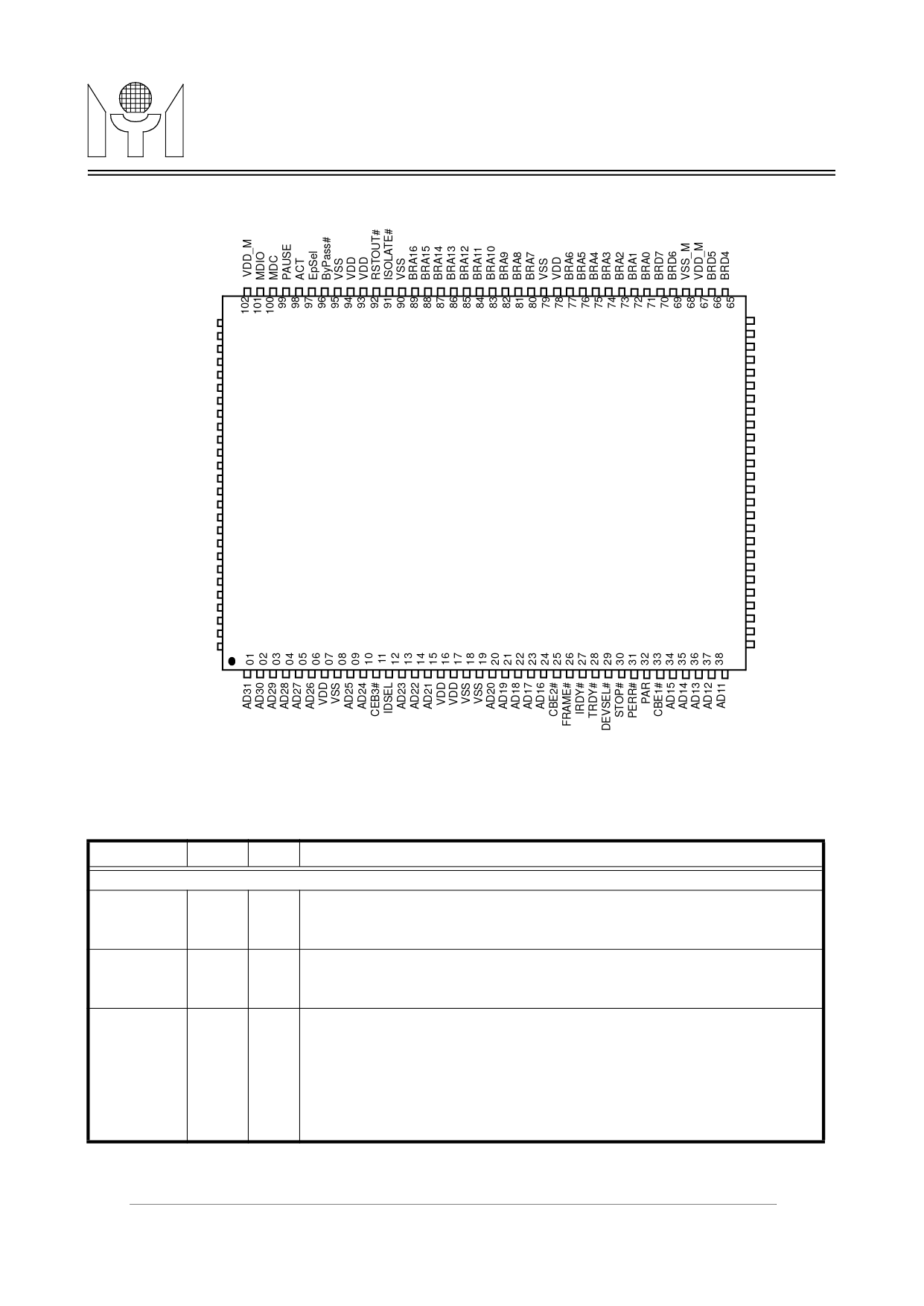
1.0 PIN CONNECTION
128 pin QFP
VSS_M 103
COL 104
CRS 105
RXER 106
RXD3 107
RXD2 108
RXD1 109
RXD0 110
RXCK 111
VDD 112
VSS 113
TXEN 114
TXD3 115
TXD2 116
TXD1 117
TXD0 118
TXCK 119
RXDV 120
INTA# 121
RST# 122
VDD 123
PCICLK 124
VSS 125
GNT# 126
REQ# 127
PME# 128
MTD800
MTD 800
(Preliminary)
64 TEST#
63 BRD3
62 BRD2
61 BRD1
60 BRD0
59 BRCS#
58 BRWR#
57 BRRD#
56 ECS
55 VSS
54 VDD
53 WUP/SGH
52 AD0
51 AD1
50 AD2
49 AD3
48 AD4
47 AD5
46 AD6
45 AD7
44 CBE0#
43
42
AD8
AD9
AD10
41 VDD
40 VSS
39
2.0 PIN DESCRIPTIONS
Name
PCICLK
RST#
AD[31:0]
Pin #
124
122
1 - 6,
9, 10
13 -15
20 - 24,
34 - 38,
41 - 43,
45 -52
I/O
Descriptions
PCI Bus Interface
PCICLK provides timing reference for the MTD800 related PCI transac-
I tions. All PCI signals except RST#,INTA# and PME# are sampled on the
rising edge of this clock.
When RST# is asserted, all output signals are put into tristate and all open
I drain pins are floated. This signal is asynchronous to PCICLK and have to
be asserted for at least 10 active PCI clock cycles.
32-bit multiplexed address and data bus. A bus transaction consists of an
I/O
address phase followed by one or more data phases. During the first cycle
in which the FRAME# is asserted, the AD[31:0] represents the address bus
while it is considered as a data bus during subsequent cycles.
2/42
MTD800 Revision 0.0 07/20/1999
Share Link: 