A6850 Ver la hoja de datos (PDF) - Altera Corporation
Número de pieza
componentes Descripción
Lista de partido
A6850 Datasheet PDF : 15 Pages
| |||
a6850 Asynchronous Communications Interface Adapter Data Sheet
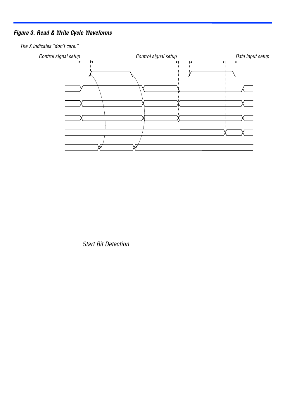
Figure 3. Read & Write Cycle Waveforms
The X indicates “don’t care.”
Control signal setup
Control signal setup
Data input setup
e
rnw X
cs X
rs X
di
do Undefined
Read
110
Valid
Valid
X
X
X
X
Write
X
110
X
Valid
X
Valid X
Undefined
Receiver Operation
Receiver operation includes the following functions:
s Start bit detection
s Data bit sampling
s Parity & stop bit detection
s Error detection
s Receive data register transfer
Start Bit Detection
The a6850 begins receiving data when a start bit is detected. A start bit is
a logic low over the rxdata input, and is sampled on each rising edge of
the rxclk signal. Once the a6850 detects a logic low, it begins counting
the logic low samples according to the specified divide-by mode (i.e., -1,
-16, or -64).
For example, after detecting a logic low in divide-by-1 mode, the a6850
assumes the next rising edge is data. After detecting a logic low in divide-
by-16 mode, however, the a6850 counts 8 clock edges and samples again.
The data must still be a logic low. At this point, the a6850 assumes the
data and clock are synchronized, and samples data every 16 clock edges
thereafter. Divide-by-64 mode is similar to divide-by-16, with the logic
low sampled at the first rising edge and the 32nd rising edge of rxclk.
Data is then sampled every 64 rising edges.
90
Altera Corporation
Share Link: 