A6850 Ver la hoja de datos (PDF) - Altera Corporation
Número de pieza
componentes Descripción
Lista de partido
A6850 Datasheet PDF : 15 Pages
| |||
a6850 Asynchronous Communications Interface Adapter Data Sheet
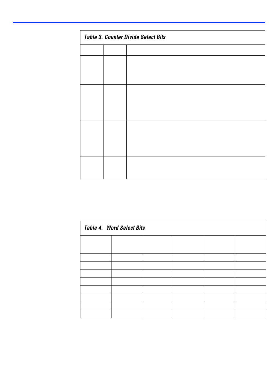
Table 3. Counter Divide Select Bits
cds1
0
0
1
1
cds0
0
1
0
1
Function
Divide-by-1 mode. Clock and data rate are identical. External
logic is responsible for synchronizing rxdata to rxclk. The
rxdata signal is sampled on the rising edge of rxclk, and
the txdata signal is asserted on the falling edge of txclk.
Divide-by-16 mode. The clock rate is 16 times the data rate.
After start bit detection (rxdata low), the rxdata signal is
sampled on the 9th rising edge of rxclk. After writing to the
transmitter data register, the txdata signal is asserted on
the first falling edge of txclk and every 16 clocks thereafter.
Divide-by-64 mode. The clock rate is 64 times the data rate.
After start bit detection (rxdata low), the rxdata signal is
sampled on the 33rd rising edge of rxclk. After writing to the
transmitter data register, the txdata signal is asserted on
the first falling edge of txclk and every 64 clocks thereafter.
Master reset. When master reset is selected, the a6850 is
reset to a known state; the status register is cleared, and the
transmit and receive operations are halted and initialized.
Word Select
Bits 2, 3, and 4 of the control register are the ws bits, which determine the
word length, parity, and number of stop bits. See Table 4.
Table 4. Word Select Bits
ws2
ws1
ws0
0
0
0
0
0
1
0
1
0
0
1
1
1
0
0
1
0
1
1
1
0
1
1
1
Word
Length
7
7
7
7
8
8
8
8
Stop Bits
2
2
1
1
2
1
1
1
Parity
Even
Odd
Even
Odd
None
None
Even
Odd
Altera Corporation
85
Share Link: 