LAN91C110 Ver la hoja de datos (PDF) - SMSC -> Microchip
Número de pieza
componentes Descripción
Lista de partido
LAN91C110 Datasheet PDF : 56 Pages
| |||
FEAST Fast Ethernet Controller for PCMCIA and Generic 16-Bit Applications
Datasheet
BRODCAST - Receive frame was broadcast.
BADCRC - Frame had CRC error, or RX_ER was asserted during reception.
ODDFRM - This bit when set indicates that the received frame had an odd number of bytes.
TOOLNG - Frame length was longer than 802.3 maximum size (1518 bytes on the cable).
TOOSHORT - Frame length was shorter than 802.3 minimum size (64 bytes on the cable).
HASH VALUE - Provides the hash value used to index the Multicast Registers. Can be used by receive routines to speed
up the group address search. The hash value consists of the six most significant bits of the CRC calculated on the
Destination Address, and maps into the 64 bit multicast table. Bits 5,4,3 of the hash value select a byte of the multicast
table, while bits 2,1,0 determine the bit within the byte selected. Examples of the address mapping:
ADDRESS
ED 00 00 00 00 00
0D 00 00 00 00 00
01 00 00 00 00 00
2F 00 00 00 00 00
HASH VALUE 5-0
000 000
010 000
100 111
111 111
MULTICAST TABLE BIT
MT-0 bit 0
MT-2 bit 0
MT-4 bit 7
MT-7 bit 7
MULTCAST - Receive frame was multicast. If hash value corresponds to a multicast table bit that is set, and the address
was a multicast, the packet will pass address filtering regardless of other filtering criteria.
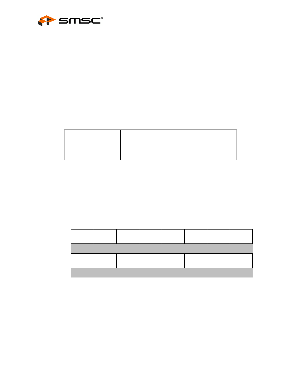
I/O SPACE
The base I/O space is specified by the power-up I/O Base Register default. To limit the I/O space requirements to 16
locations, the registers are assigned to different banks. The last word of the I/O area is shared by all banks and can be
used to change the bank in use. Registers are described using the following convention:
OFFSET
NAME
TYPE
SYMBOL
HIGH
bit 15
bit 14
bit 13
bit 12
bit 11
bit 10
bit 9
bit 8
BYTE
X
X
X
X
X
X
X
X
LOW
bit 7
bit 6
bit 5
bit 4
bit 3
bit 2
bit 1
bit 0
BYTE
X
X
X
X
X
X
X
X
OFFSET - Defines the address offset within the IOBASE where the register can be accessed at, provided the bank select
has the appropriate value.
The offset specifies the address of the even byte (bits 0-7) or the address of the complete word.
The odd byte can be accessed using address (offset + 1).
Some registers (like the Interrupt Ack., or like Interrupt Mask) are functionally described as two eight bit registers, in that
case the offset of each one is independently specified.
SMSC LAN91C110 Rev. B
Page 17
DATASHEET
Revision 1.0 (11-04-08)
Share Link: 