CB55000 Ver la hoja de datos (PDF) - STMicroelectronics
Número de pieza
componentes Descripción
Lista de partido
CB55000 Datasheet PDF : 15 Pages
| |||
CB55000 Series
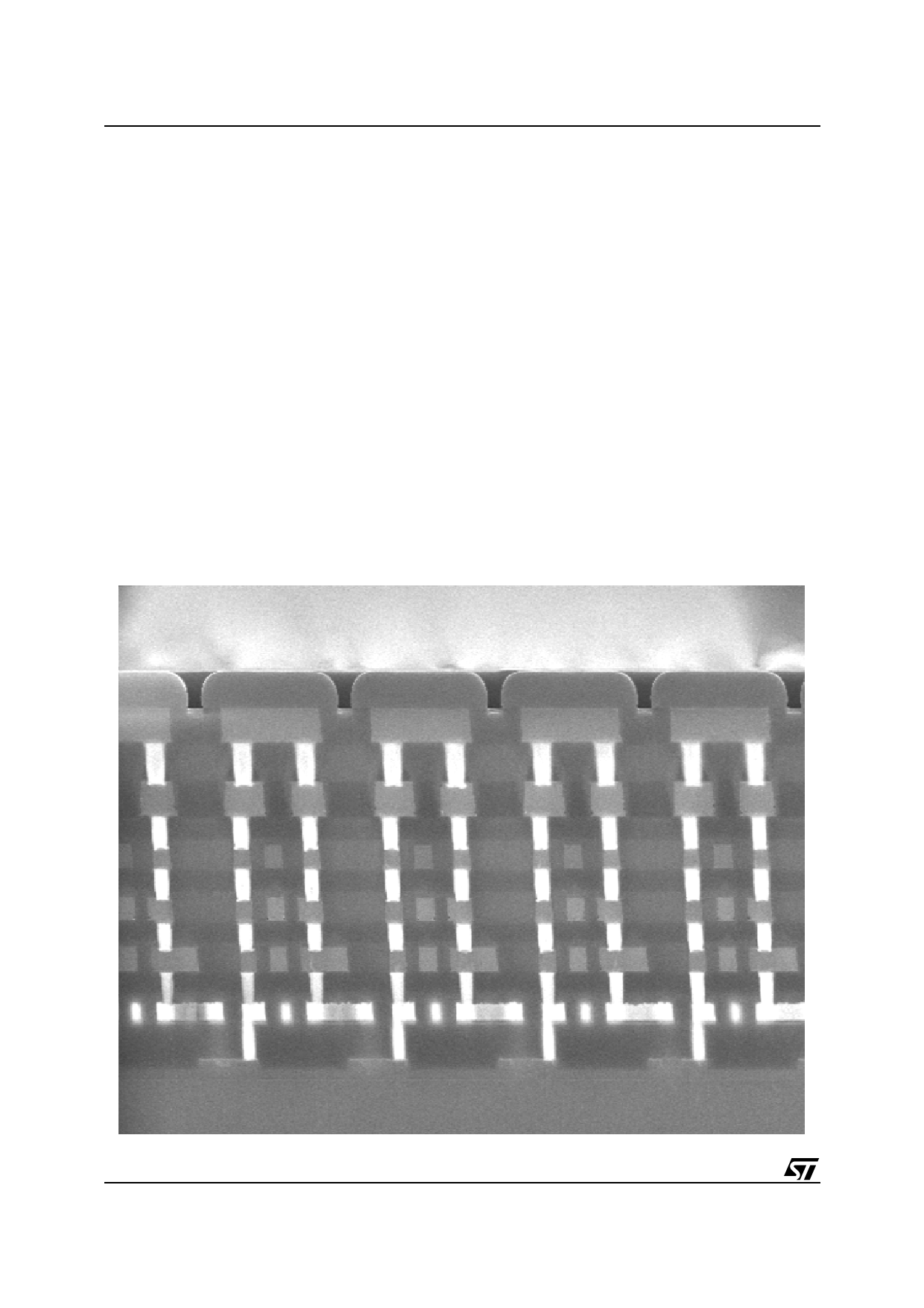
2 TECHNOLOGY OVERVIEW
The advanced HCMOS7 transistor architecture: at 0.25 µm drawn length and 0.20 µm effective length, very thin
gate oxide: 5 nanometers, optimized threshold voltages and salicided source, drain, and gate leads to intrinsi-
cally high performances in both N channel and P channel driving currents.
The major scaling factor is obtained through deep UV lithography at most masking levels, making sub-micron
pitch a reality.
Further integration in the process front-end comes from the use of the Shallow Trench Isolation process be-
tween active regions, both improving density and planarity of transistors. In order to allow full utilization of such
transistor density, up to 6 levels of metal are made available for routing.
The first metal level is Tungsten for local interconnection, while the other five metal levels are of low resistivity
aluminum for long range interconnection and power distribution.
The thick inter-level dielectric is completely planarized by Chemical Mechanical Polishing, which provides de-
fect-free isolation between stripes within the same as well as between different levels.
Usage of Tungsten plugs at contacts and vias allows extremely dense and reliable interconnection between
metal layers. These vias and contacts are fully stackable, providing a direct vertical electrical connection from
the active level up to the sixth metal level. This efficient interconnect scheme makes routing fast and easy, as
well as having a very positive impact on high gate count, random-logic blocks density and routability.
The combination of both high drive and dense transistors, easily interconnected with up to six fine-pitch metal
levels and isolated by thick dielectric leads to an optimum gate density, with low parasitic resistance and capac-
itance. This results in very short interconnected gate delay and minimized power consumption.
Figure 3. HCMOS7 Back end Cross Section
4/15
Share Link: 