CB55000 Ver la hoja de datos (PDF) - STMicroelectronics
Número de pieza
componentes Descripción
Lista de partido
CB55000 Datasheet PDF : 15 Pages
| |||
CB55000 Series
3.2 Core Logic
The propagation delays shown in CB55000 data book are given for nominal processing, 2.5 V, 25°C tempera-
ture. However, there are additional factors that affect the delay characteristics of the cells. These include: load-
ing due to fanout and interconnect routing, supply voltage, junction temperature of the device, processing
tolerance and input signal transition time.
Prior to physical layout, the design system can estimate the delays associated with any critical path. The impact
of the placement and routing can be accurately RC back-annotated from the layout for final simulations of critical
timing. The median effects on the cells delay of junction temperature (Kt coefficient) and supply voltage (Kv co-
efficient) are summarized in the following tables at a fixed cell input slope. A third factor is related to process
variations and has a minimum median of 0.84 for best case process and a maximum median of 1.18 for worst
case process.
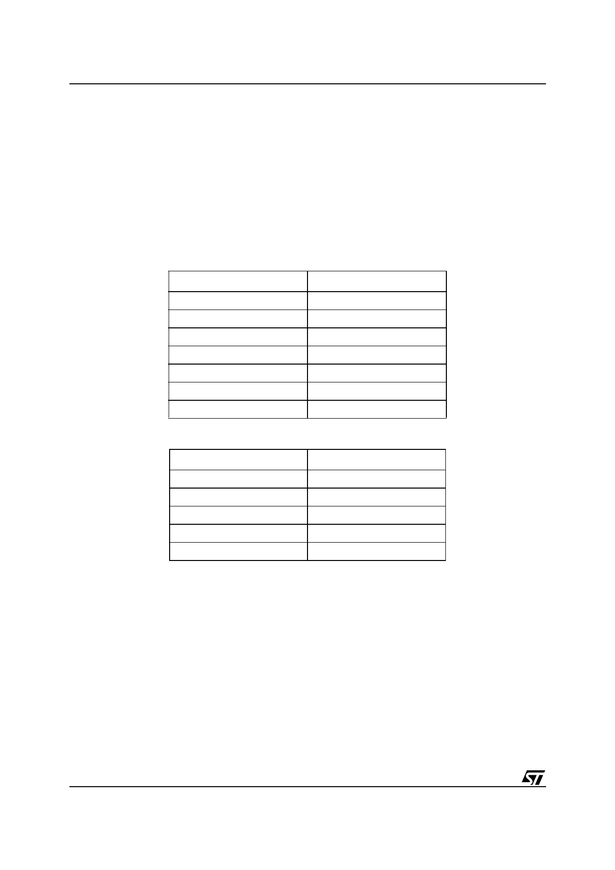
Table 1. Junction temperature multipliers
Temperature (°C)
Kt
-55
.84
-40
.87
25
1.00
70
1.09
85
1.12
105
1.16
125
1.20
Table 2. Voltage multipliers
Vdd (V)
Kv
1.80
1.33
2.00
1.21
2.25
1.09
2.50
1.00
2.75
0.94
3.3 I/O Buffer Libraries
Two basic buffer libraries are offered with CB55000, one 80 µm pad in line pitch library and one 50 µm stag-
gered pad library to support pad limited designs.
Apart from standard ESD and latch-up protections present in each I/O, a proprietary clamp within each power
supply provides proper paths to all types of ESD discharges, efficiently protecting the I/Os. As a result, the buff-
ers withstand more than 4 kV ESD according to Mil 883C Human Body Model specification.
In order to limit switching noise and keep a fixed buffer delay, independent of process, supply voltage and tem-
perature, compensated active slew rate buffers can be selected, providing a fixed and stable dI/dt at 8,16 or
32 mA/ns.
In order to interface with 3.3 V application (from 2.7 up to 3.6 V), a wide range of 3.3 V capable input/output
buffers (mixable with standard 2.5V ones) can be chosen. In this case the 3.3 V rail in the chip periphery must
be powered through a 3.3 V external supply.
True 5 volt tolerant input buffer is also available with process option.
6/15
Share Link: 